What Is an IoT IC Test PCB?
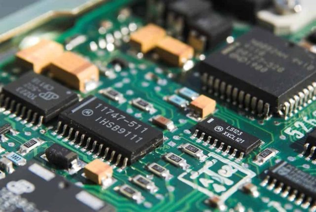
An IoT IC Test PCB is a specialized printed circuit board used for validating and testing integrated circuits (ICs) designed for Internet of Things (IoT) applications. These PCBs are commonly used in semiconductor test environments such as:
-
Automated Test Equipment (ATE) systems
-
Load boards
-
Probe card assemblies
-
Burn-in testing platforms
IoT chips often integrate RF modules, low-power processors, memory, and sensor interfaces into compact packages, requiring precise and reliable test boards.
Key Requirements of IoT IC Test PCB
1. Support for Low Power and High Integration Chips
IoT ICs typically feature:
-
Ultra-low power consumption
-
High integration (MCU + RF + Memory)
-
Compact package formats
-
Mixed signal architecture
The test PCB must provide stable power distribution and minimal electrical noise to ensure accurate test results.
2. Controlled Impedance for RF and High-Speed Signals
Many IoT chips support wireless communication protocols such as:
-
Wi-Fi
-
Bluetooth
-
Zigbee
-
LoRa
-
NB-IoT
The IoT IC Test PCB must support:
-
50Ω RF transmission lines
-
Differential pair routing
-
Low loss materials for RF paths
-
Stable impedance control
Signal integrity is essential for validating RF performance.
3. High Pin Count and Fine Pitch Capability
IoT IC packages may include:
-
QFN
-
BGA
-
WLCSP
-
Fine pitch LGA
The PCB must support:
-
Fine line and spacing
-
Via-in-pad design
-
Microvia structures
-
High layer count routing
This ensures reliable electrical connections during test operations.
4. Thermal and Reliability Performance
In production testing and burn-in environments, boards may experience:
-
Continuous operation
-
Elevated temperatures
-
Repeated mechanical insertion cycles
IoT IC Test PCB should feature:
-
High TG materials
-
Strong pad adhesion
-
Stable copper thickness
-
Reliable plating quality
This ensures long-term durability and consistent performance.
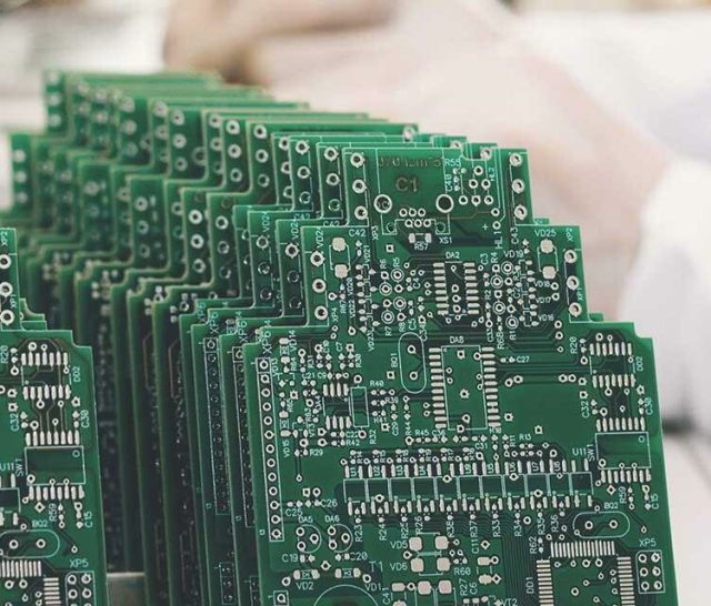
Manufacturing Capabilities for IoT IC Test PCB
Advanced fabrication may include:
-
4–16+ layer stack-ups
-
Controlled impedance processing
-
Laser drilled microvias
-
Sequential lamination
-
ENIG or ENEPIG surface finish
-
High density routing
-
Tight tolerance fabrication
Strict quality control ensures stable electrical characteristics.
Applications of IoT IC Test PCB
IoT IC Test PCB is widely used for testing chips in:
-
Smart home devices
-
Wearable electronics
-
Industrial IoT systems
-
Smart meters
-
Automotive IoT modules
-
Environmental sensors
-
Edge computing devices
As IoT deployment expands globally, reliable semiconductor testing becomes increasingly critical.
Why Choose a Professional IoT IC Test PCB Manufacturer
An experienced supplier should provide:
-
Expertise in semiconductor test board fabrication
-
RF and mixed-signal PCB experience
-
High density routing capability
-
Stable material sourcing
-
Fast prototype and small batch production
-
Strict quality inspection
Reliable manufacturing ensures accurate test data and stable chip validation.
Conclusion
IoT IC Test PCB plays a crucial role in validating modern low power and RF-enabled semiconductor devices. With controlled impedance design, high density routing, and robust material selection, these PCBs support accurate, stable, and efficient chip testing environments.
Partnering with a professional PCB manufacturer ensures high quality, consistent performance, and fast delivery for IoT semiconductor projects.
