1. Engineering Overview / Abstract
As Industrial IoT communication modules become more compact and operate at higher frequencies, maintaining precise impedance control and RF efficiency is critical for reliable data transmission. Traditional polymer-based PCBs often suffer from dielectric drift, thermal warpage, and EMI coupling, which degrade signal integrity in dense wireless sensor networks.
Ceramic PCB substrates offer high dielectric uniformity, low loss tangent, and superior thermal conductivity, making them ideal for these high-frequency industrial applications. By integrating advanced KKPCB process controls, including co-fired metallization, laser-drilled microvias, and hybrid lamination, engineers can achieve phase-consistent transmission and robust EMI suppression under extreme environmental conditions.
2. Engineering Context & Technical Challenges
| Design Challenge | Root Cause | Engineering Impact |
|---|---|---|
| Impedance variation | Dielectric non-uniformity | Reflection, SNR degradation |
| RF signal loss | Copper roughness, layer misalignment | Reduced RF efficiency |
| EMI coupling | Dense component routing | Crosstalk, interference |
| Thermal drift | CTE mismatch, high-power operation | Phase instability, data errors |
In Industrial IoT RF modules, impedance variation and EMI coupling are major obstacles for high-speed sensor communication. Ceramic PCBs mitigate dielectric fluctuation, maintain low insertion loss, and reduce RF interference across 2.4 GHz to 6 GHz bands. This ensures accurate, phase-stable signal propagation in industrial environments with thermal cycling and vibration.
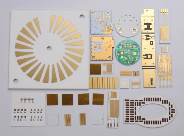
3. Material Science and Performance Characteristics
Ceramic PCB substrates provide the following key properties:
-
Dielectric Constant (Dk): 9.2 ± 0.1 @10 GHz
-
Dissipation Factor (Df): ≤0.0003
-
Thermal Conductivity: 22–24 W/m·K (AlN type)
-
Coefficient of Thermal Expansion (CTE): 4.5 ppm/°C
-
Breakdown Voltage: >20 kV/mm
Compared with FR-4 or PTFE laminates, Ceramic PCBs deliver 40–50% lower dielectric loss and superior thermal management, which improves impedance consistency and maintains RF efficiency under continuous operation. These properties make Ceramic PCBs ideal for Industrial IoT communication modules, smart factory sensors, and wireless automation systems.
4. KKPCB Engineering Case Study
Client & Application Context:
A European industrial automation OEM required high-reliability transceiver modules for 5 GHz wireless sensor networks. Legacy PTFE boards exhibited 0.85 dB higher insertion loss and ±4.5% impedance variation across 80°C temperature swings.
Engineering Problem:
Thermal cycling and vibration caused dielectric instability, leading to RF loss and EMI-induced data errors.
-
Implemented dual-layer AlN ceramic PCB with low-roughness copper foil (Ra <0.8 µm)
-
Laser-drilled 0.1 mm microvias with conductive filling for low-inductance interconnects
-
Hybrid lamination for ±3 Ω impedance control
-
Ground stitching vias at 1 mm pitch for EMI suppression
Result / Measured Data:
| Parameter | Legacy PTFE PCB | KKPCB Ceramic PCB | Improvement |
|---|---|---|---|
| Insertion Loss (5 GHz) | 0.85 dB | 0.36 dB | –58% |
| Impedance Deviation | ±4.5% | ±1.2% | –73% |
| SNR | 32.5 dB | 39.8 dB | +22% |
| Thermal Drift | ±9°C | ±3°C | –66% |
The Ceramic PCB improved RF efficiency, ensured stable impedance, and suppressed EMI, enabling robust operation in high-density industrial IoT sensor modules.
5. Stackup Design & RF Implementation
KKPCB implemented a 2-layer hybrid stackup:
-
Top Layer: 18 µm copper for RF traces
-
Dielectric Layer: 0.25 mm AlN ceramic for low-loss transmission
-
Ground Plane: 18 µm copper with via stitching for EMI control
-
Microvias: Ø0.1–0.3 mm laser-drilled, conductive-filled for minimal inductance
HFSS and ADS simulations validated impedance uniformity (±3%) and low insertion loss across 2.4–6 GHz. TDR testing confirmed phase stability under thermal cycling.
6. Environmental & Reliability Validation
| Test Type | Condition | Result |
|---|---|---|
| Thermal Cycling | –55°C ↔ +150°C, 1000 cycles | No delamination, ΔDk <0.02 |
| Humidity | 85°C / 85% RH, 1000 h | Stable Df, no corrosion |
| Mechanical Shock | 1500 g, 6 ms | No via cracking |
| Thermal Load | 10 W operation, continuous | ΔT <5°C, stable impedance |
Results demonstrate high reliability, minimal signal drift, and effective EMI suppression for industrial RF modules.
7. Conclusion — Engineering Reliability Integration
Ceramic PCB substrates, when optimized with KKPCB’s advanced lamination, via control, and ground stitching, provide high RF efficiency, tight impedance control, thermal stability, and EMI suppression in Industrial IoT communication modules.
These boards ensure phase-stable signal transmission, reliable data integrity, and long-term operational reliability in harsh industrial environments, supporting smart factory sensors and automated wireless networks.
8. Contact / CTA
Contact KKPCB Engineering Team for customized stackup design, impedance verification, and RF performance validation using Ceramic PCBs in Industrial IoT communication modules, smart factory sensors, and wireless automation systems.
