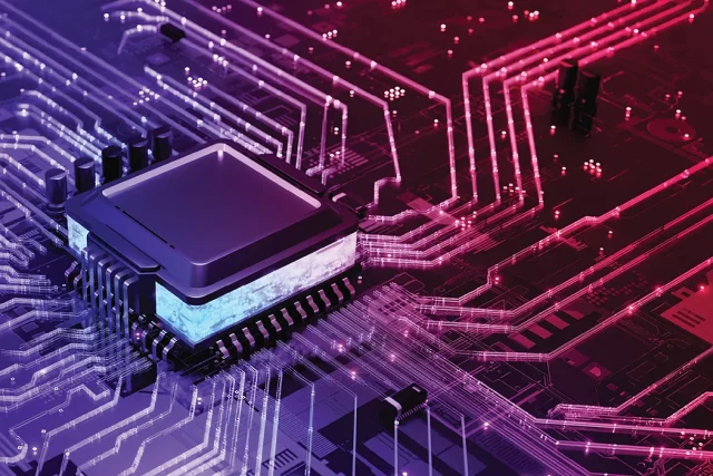
As data rates continue to increase, validating high-speed digital interfaces requires test platforms that introduce minimal distortion. The High Speed Test PCB is engineered to act as a transparent signal medium, enabling accurate characterization of high-speed devices and systems.
A well-designed high speed test PCB ensures that test results reflect real device performance rather than PCB-induced errors.
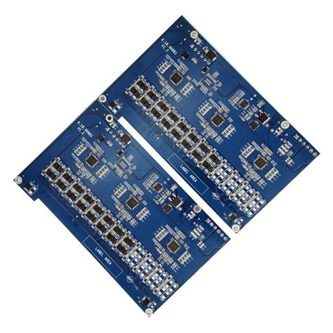
What Is a High Speed Test PCB?
A High Speed Test PCB is a test-focused printed circuit board optimized for validating high-speed digital signals such as SerDes, DDR, PCIe, USB, and Ethernet. Unlike RF-oriented test boards, it emphasizes timing accuracy and signal fidelity in the time domain.
Why High Speed Test PCBs Are Essential
High-speed testing demands:
-
Minimal signal distortion and attenuation
-
Tight control of skew and jitter
-
Repeatable electrical behavior across test cycles
High speed test PCBs provide a stable and predictable test environment.
Controlled Impedance and Differential Pair Design
Accurate impedance control is fundamental. High speed test PCBs focus on:
-
Tight tolerance single-ended and differential impedance
-
Matched differential pair geometry
-
Stable reference planes
Consistent impedance ensures clean eye diagrams and BER results.
Length Matching and Timing Control
Timing accuracy is critical at high data rates. High speed test PCBs use:
-
Precise trace length matching
-
Symmetrical routing paths
-
Delay tuning where necessary
These techniques minimize skew and timing mismatch.
Low-Loss Materials for High-Speed Digital Signals
Material selection affects signal quality. High speed test PCBs may use:
-
Low-Df laminates to reduce attenuation
-
Smooth copper foil for reduced conductor loss
-
Hybrid stackups balancing cost and performance
Low-loss materials improve signal margin.
Via Design and Signal Transitions
Vias can introduce discontinuities. High speed test PCBs mitigate this by:
-
Short via stubs or back-drilling
-
Optimized via pad and anti-pad design
-
Grounded return vias near signal transitions
Clean transitions preserve eye opening.
Crosstalk and Noise Suppression
Dense high-speed routing increases coupling risk. Effective solutions include:
-
Adequate spacing between signal channels
-
Ground stitching and reference continuity
-
Isolation between noisy and sensitive signals
Noise control ensures repeatable test results.
Manufacturing Precision and Electrical Verification
High speed test PCBs require:
-
Tight process tolerances
-
Impedance coupon testing
-
Electrical and signal verification
Manufacturing accuracy directly impacts test reliability.
Typical Applications of High Speed Test PCBs
High speed test PCBs are commonly used in:
-
High-speed interface validation
-
Semiconductor characterization
-
Data center and networking hardware testing
-
Functional and compliance testing platforms
Each application depends on consistent signal behavior.
Selecting a High Speed Test PCB Manufacturer
When choosing a high speed test PCB supplier, look for:
-
Experience with high-speed digital designs
-
Controlled impedance and low-loss fabrication capability
-
Support for prototype and engineering builds
-
Understanding of test-driven design requirements
An experienced partner helps ensure accurate validation.
Conclusion
The High Speed Test PCB is a critical tool for validating modern high-speed digital systems. Through controlled impedance, precise timing control, and low-loss design, high speed test PCBs enable accurate, repeatable, and trustworthy test results.
Partnering with a specialized high speed test PCB manufacturer ensures reliable performance in demanding validation environments.
