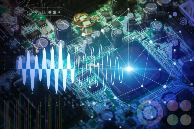
A High Speed IC Test PCB is a specialized printed circuit board designed to support high-frequency, high-data-rate, and fast edge-rate integrated circuit testing. As modern ICs operate at GHz-level frequencies and multi-gigabit data rates, traditional PCB designs are no longer sufficient to guarantee accurate test results.
High speed IC test PCBs are widely used in Automated Test Equipment (ATE), load boards, probe card interfaces, and IC characterization platforms, where signal integrity, timing accuracy, and repeatability are critical.
Key Design Challenges in High Speed IC Test PCBs
1. Signal Integrity at High Data Rates
High-speed IC testing requires controlled impedance traces, minimal impedance discontinuities, and precise length matching. Even small routing inconsistencies can cause signal reflections, jitter, and eye-diagram degradation, leading to incorrect test measurements.
2. Crosstalk and Noise Control
Dense routing and high pin count ICs increase the risk of near-end and far-end crosstalk. High speed IC test PCBs must use proper spacing rules, reference planes, and differential pair routing techniques to maintain clean signals.
3. Power Integrity for Fast-Switching ICs
High-speed ICs generate rapid current transients. A robust power distribution network (PDN) with low-inductance planes, dense decoupling capacitors, and short return paths is essential for stable test conditions.
4. Timing and Skew Control
In high speed digital testing, timing margin is extremely tight. Controlled trace lengths, matched differential pairs, and consistent via structures are required to ensure accurate timing alignment across all test channels.
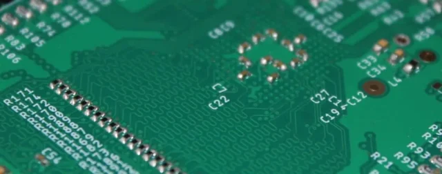
Structural Features of High Speed IC Test PCBs
A professional high speed IC test PCB typically includes:
-
Controlled impedance routing for single-ended and differential signals
-
Low-loss PCB materials to reduce insertion loss at high frequencies
-
Multilayer PCB stackups with dedicated signal, ground, and power planes
-
Microvias, blind vias, or buried vias to minimize parasitic effects
-
High-density layouts supporting fine-pitch and high pin count ICs
These features ensure repeatable high-speed signal performance throughout the test lifecycle.
Applications of High Speed IC Test PCBs
High speed IC test PCBs are essential in:
-
ATE systems and IC production test platforms
-
Load board PCBs for high-speed digital ICs
-
SerDes, memory, and processor IC testing
-
High-speed interface validation (PCIe, USB, Ethernet, DDR)
-
5G, AI, and data center IC characterization
In each application, test accuracy directly depends on PCB electrical performance.
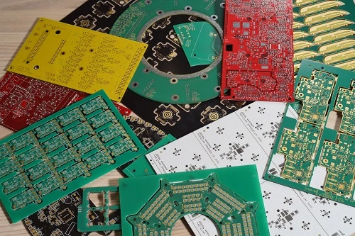
Manufacturing Requirements for High Speed IC Test PCBs
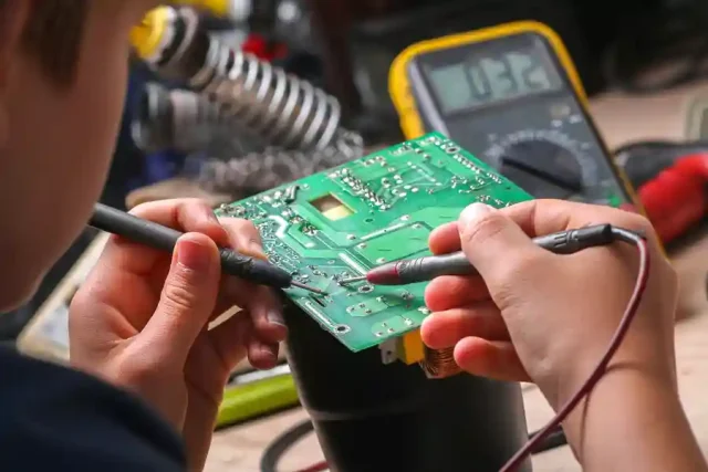
To ensure reliable performance, manufacturing a high speed IC test PCB requires:
-
Tight control of trace width, spacing, and impedance tolerance
-
Advanced multilayer lamination and registration accuracy
-
Precision drilling and consistent via plating
-
Impedance testing and electrical verification
-
Support for prototype, small batch, and volume production
An experienced PCB manufacturer can deliver high-yield, high-reliability test boards that meet demanding semiconductor test standards.
Conclusion
A High Speed IC Test PCB is a critical foundation for accurate validation of modern high-performance integrated circuits. By combining controlled impedance design, low-loss materials, robust power integrity, and advanced multilayer construction, these PCBs enable clean signal transmission, precise timing, and reliable test results.
Choosing a trusted high speed IC test PCB manufacturer helps semiconductor companies reduce test risk, improve yield, and accelerate time-to-market from engineering validation to mass production.
