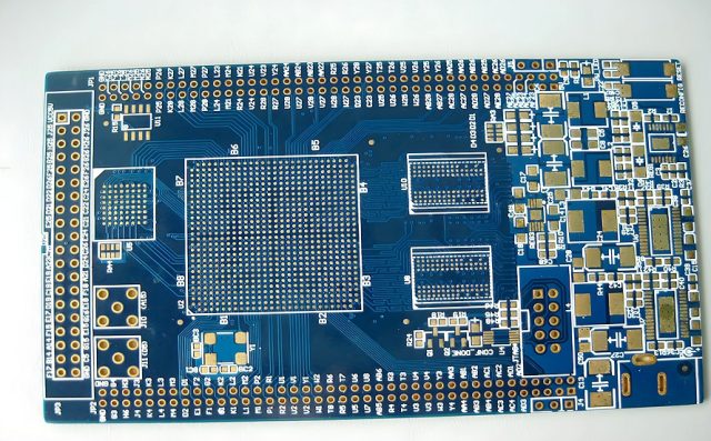
What Is a High Speed IC Test PCB?

A High Speed IC Test PCB is a specialized printed circuit board used to test integrated circuits operating at high data rates and high frequencies. It functions as the electrical interface between the device under test (DUT) and automated test equipment (ATE), ensuring accurate transmission and measurement of high-speed signals.
These PCBs are widely applied in testing high-speed digital ICs, SerDes devices, processors, memory ICs, communication chips, and other performance-critical semiconductor components.
Why High Speed IC Testing Requires Specialized PCBs
As IC operating speeds continue to increase, signal integrity becomes a major challenge during testing. High speed IC test PCBs must address issues such as:
-
Signal attenuation and insertion loss
-
Impedance discontinuities
-
Crosstalk and electromagnetic interference (EMI)
-
Timing skew and jitter
-
Power integrity at high switching speeds
A standard PCB cannot meet these requirements, making specialized high-speed test PCB design essential.
Key Requirements of High Speed IC Test PCBs
A reliable high speed IC test PCB must provide:
-
Precisely controlled impedance routing
-
Low-loss transmission lines for high-frequency signals
-
Excellent signal integrity and timing accuracy
-
Low crosstalk and noise coupling
-
Stable power distribution networks (PDN)
-
High pin count and fine-pitch support
Even small variations in PCB geometry or materials can significantly affect high-speed test results.
High Speed PCB Design Considerations
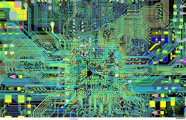
Designing a high speed IC test PCB typically involves:
-
Carefully optimized multilayer stackups
-
Dedicated high-speed signal layers with solid reference planes
-
Short, matched-length routing for critical signals
-
Controlled via structures to minimize reflections
-
Proper termination and impedance matching
-
Strategic placement of decoupling capacitors
Design accuracy directly impacts test repeatability and yield.
Materials for High Speed IC Test PCBs
Material selection plays a crucial role in high-speed performance. Common materials include:
-
Low Dk / Low Df laminates for reduced signal loss
-
High-performance FR-4 for moderate-speed applications
-
Hybrid material stackups combining low-loss cores with standard materials
-
Stable dielectric systems for impedance consistency
Choosing the right material ensures signal integrity across the required frequency range.
Manufacturing Capabilities
High speed IC test PCBs require advanced manufacturing capabilities, including:
-
Multilayer PCB fabrication (8–30+ layers)
-
Tight impedance control and verification
-
HDI technology for dense routing
-
High-precision drilling and registration
-
Premium surface finishes such as ENIG or ENEPIG
Manufacturing precision directly affects electrical performance and test reliability.
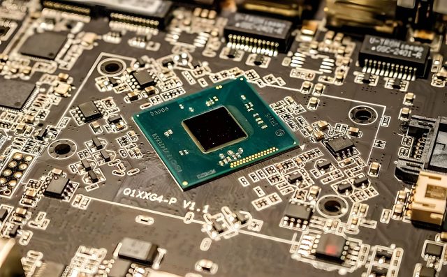
Assembly for High Speed IC Testing
Assembly quality is equally critical and often includes:
-
High-speed test sockets or DUT interfaces
-
RF or high-speed board-to-board connectors
-
Precision passive components
-
Controlled soldering processes to reduce parasitics
Poor assembly can negate even the best PCB design.
Applications of High Speed IC Test PCBs
High speed IC test PCBs are commonly used in:
-
SerDes and high-speed interface testing
-
CPU, GPU, and ASIC testing
-
High-speed memory IC validation
-
Networking and data center IC testing
-
Automotive and industrial high-speed electronics
They are essential for validating IC performance under real operating conditions.
Why Choose a Professional High Speed IC Test PCB Manufacturer
An experienced manufacturer offers:
-
Deep expertise in high-speed signal integrity
-
Proven stackup and impedance control solutions
-
Stable quality for repeated test cycles
-
Fast prototype and small batch production
-
Engineering support throughout the project lifecycle
The right partner helps reduce debug time, improve test accuracy, and accelerate time to market.
