With the rapid development of IoT, smart devices, and industrial automation, sensors are becoming increasingly important in modern electronic systems. Many advanced sensing technologies operate at high frequencies to achieve greater accuracy, faster response times, and improved detection capabilities.
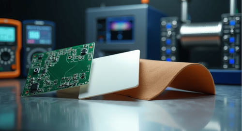
At the core of these systems lies the High Frequency Sensor PCB, which enables stable signal transmission and accurate data acquisition. Designing a reliable high frequency sensor PCB requires specialized materials, careful layout strategies, and precise manufacturing techniques.
Applications of High Frequency Sensor PCB
High frequency sensor PCBs are widely used across various industries that require accurate signal detection and processing.
Typical applications include:
-
Radar sensor modules
-
Automotive sensing systems
-
Industrial monitoring sensors
-
Wireless sensor networks
-
Medical sensing devices
-
Environmental monitoring equipment
These applications require stable RF signal transmission and high sensitivity for accurate sensing performance.
Key Technical Requirements for High Frequency Sensor PCB
1. Low-Loss High-Frequency Materials
High-frequency signals are sensitive to dielectric loss, making material selection critical in sensor PCB design.
Common materials include:
-
Rogers high-frequency laminates
-
PTFE-based materials
-
Low-loss modified FR-4
These materials help minimize signal attenuation and improve sensor accuracy.
2. Controlled Impedance Design
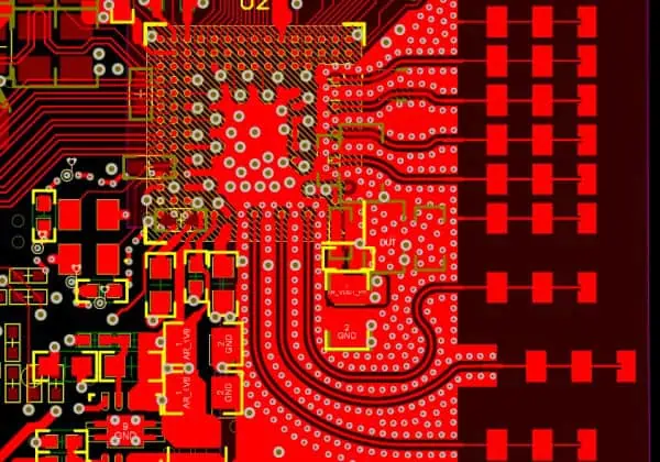
High-frequency sensor circuits require precise impedance control to maintain signal integrity.
Important design practices include:
-
Controlled impedance traces
-
Proper transmission line design
-
Differential pair routing
-
Stable reference ground planes
Accurate impedance control ensures reliable signal transmission between sensors and processing units.
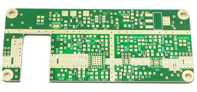
3. Compact Multilayer PCB Structures
Many sensor modules integrate RF circuits, analog signal processing, and digital communication components.
To accommodate these functions, designers often use multilayer PCB structures, which allow:
-
Efficient routing of high-speed signals
-
Reduced electromagnetic interference
-
Better signal isolation
This helps maintain stable performance in compact sensor devices.
4. Electromagnetic Interference Control
High-frequency sensor systems are sensitive to external noise and interference.
To improve electromagnetic compatibility (EMC), PCB designers use techniques such as:
-
Ground shielding structures
-
Proper signal return paths
-
Isolation between RF and digital circuits
These measures help ensure accurate sensor measurements.
5. Thermal Management
Some high-frequency sensors generate heat during operation, especially in radar or industrial sensing systems.
Effective thermal design may include:
-
Thermal vias
-
Copper heat spreading layers
-
Optimized component placement
Proper heat management improves long-term reliability.
Manufacturing Considerations for High Frequency Sensor PCB
Producing high-quality high frequency sensor PCBs requires advanced manufacturing capabilities, including:
-
Precision impedance control
-
Fine line circuit fabrication
-
High-frequency material processing
-
Strict quality control for RF performance
Reliable manufacturing ensures consistent electrical characteristics and stable sensor performance.
Conclusion
As sensing technology continues to evolve, High Frequency Sensor PCBs are playing an increasingly important role in enabling precise signal detection and reliable data transmission.
By combining advanced materials, optimized PCB design techniques, and high-precision manufacturing processes, high frequency sensor PCBs provide the foundation for next-generation sensing technologies used in automotive systems, industrial monitoring, and IoT devices.
