What Is a High Current PCB?
A High Current PCB is a printed circuit board specifically designed to carry large currents while maintaining electrical stability and thermal reliability. These PCBs are commonly used in power electronics, automotive inverters, industrial automation, renewable energy systems, and high-current semiconductor testing.
High current PCBs typically feature thick copper layers, wider traces, and optimized thermal dissipation structures to prevent overheating and ensure stable operation.
Why High Current PCB Technology Matters
As electronic systems demand higher power densities and reliability, standard PCBs may fail under high current conditions. High current PCBs address challenges such as:
-
Excessive voltage drop on power traces
-
Thermal buildup and hotspots
-
Mechanical stress due to heavy copper layers
-
Signal integrity for high-power switching circuits
-
Reliability under repetitive current cycling
Proper design and manufacturing are critical to ensure long-term performance and safety.
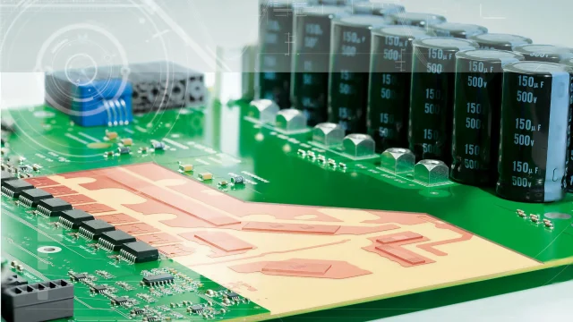
Key Features of High Current PCBs
A high-quality high current PCB includes:
-
Thick copper layers (up to 6 oz or more per layer)
-
Wide power traces and planes
-
Optimized via structures for current distribution
-
Thermal relief and heat dissipation strategies
-
High TG substrates for thermal stability
These features allow the PCB to handle large currents without overheating or reliability issues.
Design Considerations for High Current PCBs
Designing a high current PCB requires careful attention to:
-
Copper thickness and trace width calculation
-
Multilayer power distribution design
-
Via-in-pad and multiple via arrays for current sharing
-
Thermal vias and heat sinks integration
-
Mechanical reinforcement for heavy copper layers
A robust design ensures safe operation in power-intensive applications.
Materials Used in High Current PCBs
Material selection is essential for handling high currents:
-
High-TG FR-4 for thermal stability
-
Heavy copper laminates for large current capacity
-
Polyimide and composite substrates for high-temperature applications
-
Low-loss laminates if high-frequency signals coexist
-
Metal core PCB options for efficient heat dissipation
Choosing the right material ensures long-term electrical and mechanical performance.
Manufacturing Capabilities for High Current PCBs
High current PCB fabrication requires specialized capabilities:
-
Heavy copper lamination (up to 12 oz or more per layer)
-
Accurate etching for wide and thick traces
-
Precise via filling and plating for current distribution
-
Thermal analysis and layer-to-layer registration control
-
Rigorous AOI, electrical testing, and thermal testing
Advanced manufacturing ensures consistent performance under high current stress.
Assembly Considerations for High Current PCBs
Assembly of high current PCBs includes:
-
Soldering high-current components with optimized thermal profiles
-
Heavy-duty connectors and busbars integration
-
Thermal interface materials for heat dissipation
-
Quality inspection for current-carrying traces
-
Functional testing under full load conditions
Proper assembly is crucial to preserve high current performance.
Applications of High Current PCBs
High current PCBs are widely used in:
-
Power converters and inverters
-
Electric vehicles (EV) and hybrid EVs
-
Industrial automation and robotics
-
Renewable energy systems (solar inverters, wind energy)
-
High current semiconductor test boards
-
Aerospace and defense power systems
They are essential wherever large currents must be handled safely and reliably.
Why Choose a Professional High Current PCB Manufacturer
A professional high current PCB manufacturer provides:
-
Expertise in thick copper and heavy current designs
-
Stable quality for industrial and automotive applications
-
Thermal and mechanical optimization for safety
-
Prototypes and small batch production support
-
One-stop PCB fabrication and assembly services
The right partner ensures high reliability, safe power handling, and consistent performance under demanding conditions.
