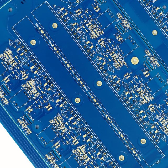
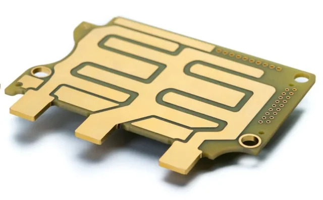
As modern electronic systems demand higher power and greater reliability, Heavy Copper PCB technology has become essential for applications requiring high current carrying capacity and enhanced thermal performance. Heavy copper PCBs are designed with thicker copper layers than standard PCBs, allowing them to handle large electrical currents while maintaining structural stability and heat dissipation.
These circuit boards are widely used in industries such as power electronics, automotive systems, industrial control, and renewable energy equipment.
What Is a Heavy Copper PCB?
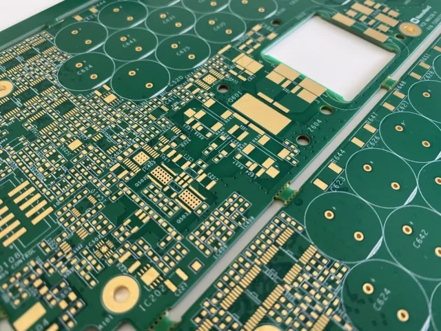
A Heavy Copper PCB is a printed circuit board that uses copper thickness typically greater than 3 oz/ft² (105 µm) and can reach 20 oz or more depending on the application. The thick copper layers allow the PCB to support high current loads and improve heat dissipation across the board.
Compared with standard PCBs that usually use 1 oz or 2 oz copper, heavy copper PCBs offer significantly improved electrical and thermal performance.
Advantages of Heavy Copper PCBs
1. High Current Carrying Capacity
The thicker copper layers allow heavy copper PCBs to safely handle large currents without overheating.
2. Improved Thermal Management
Heavy copper traces help distribute and dissipate heat more effectively, improving system stability.
3. Increased Mechanical Strength
Thick copper layers enhance the durability of the PCB and improve resistance to mechanical stress.
4. Enhanced Reliability
Heavy copper PCBs reduce the risk of trace failure in high-power circuits, ensuring long-term reliability.
5. Compact High-Power Designs
Engineers can integrate high-current circuits into smaller board designs without sacrificing safety or performance.
Design Considerations for Heavy Copper PCB
Designing a Heavy Copper PCB requires special attention to several key factors:
-
Proper trace width and spacing for high current flow
-
Thermal management strategies such as heat sinks or thermal vias
-
Controlled impedance if high-speed signals are also present
-
Careful PCB stack-up planning for multilayer power boards
-
Compatibility with manufacturing processes for thick copper plating
Working closely with an experienced PCB manufacturer is essential for achieving reliable heavy copper PCB designs.
Applications of Heavy Copper PCB
Heavy copper PCBs are widely used in high-power electronic systems, including:
-
Power supply units
-
Industrial motor controllers
-
Electric vehicle power systems
-
Solar inverters and renewable energy equipment
-
Battery management systems
-
Power distribution equipment
These applications require circuit boards capable of safely handling high current and maintaining stable thermal performance.
Manufacturing Challenges
Fabricating heavy copper PCBs requires specialized manufacturing processes due to the increased copper thickness. Key considerations include:
-
Advanced copper plating technology
-
Precise etching processes for thick copper layers
-
Reliable drilling and plating for vias
-
Careful thermal stress management during production
These processes ensure the final PCB maintains both electrical performance and structural integrity.
Conclusion
Heavy Copper PCB technology provides an effective solution for high-power electronic applications requiring high current capacity, improved thermal management, and long-term reliability. By incorporating thick copper layers and optimized PCB designs, heavy copper PCBs enable efficient power distribution in demanding industries such as automotive, renewable energy, and industrial automation.
