Engineering High Layer Count PCBs: Why “More Layers” Isn’t the Answer

As electronic systems evolve toward higher speeds, higher integration, and smaller form factors, high layer count PCBs—typically 16 layers and above—have become standard in data centers, telecommunications, aerospace electronics, and advanced industrial systems.
However, many multilayer PCBs fail not because of schematic errors, but because stackup planning and lamination control were treated as afterthoughts. At KKPCB, we approach high layer count PCB design as a system-level engineering challenge, where electrical, mechanical, and manufacturing disciplines must align from day one.
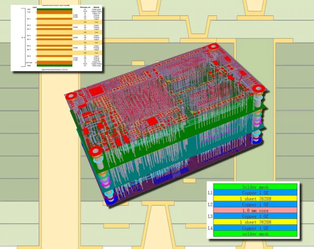
Stackup Planning: The Core of Multilayer PCB Performance
Signal Integrity Begins with the Stackup
In high layer count PCBs, signal integrity is defined by stackup architecture. Proper stackup planning ensures:
-
Stable impedance across all high-speed signal layers
-
Continuous and predictable return current paths
-
Reduced crosstalk and electromagnetic interference
-
Lower insertion loss at multi-gigabit data rates
KKPCB engineers prioritize signal–reference–signal symmetry, ensuring that every critical trace is tightly coupled to a solid reference plane. This approach is essential for high-speed digital buses, SerDes channels, and RF signal paths.
Power Integrity Is Engineered into the Layer Structure
As current density increases, power integrity becomes a limiting factor. Well-designed high layer count PCB stackups integrate:
-
Closely spaced power and ground planes
-
Distributed plane capacitance
-
Short, low-inductance current loops
This stackup-driven power integrity strategy reduces voltage ripple, improves transient response, and enhances overall system stability.
Material Selection: Controlling Loss, Stability, and Yield
Material behavior becomes increasingly critical as layer count rises. Resin flow, dielectric thickness variation, and thermal expansion mismatch can all compromise reliability.
KKPCB evaluates PCB materials based on:
-
Dielectric constant (Dk) and dissipation factor (Df) stability
-
Z-axis expansion and CAF resistance
-
Compatibility with multiple lamination cycles
-
Long-term thermal and mechanical stability
For mixed-signal or RF-digital hybrid designs, hybrid stackups are carefully engineered to ensure consistent performance without introducing lamination or registration risks.
Sequential Lamination: Necessary but Risk-Sensitive
High layer count PCBs often require sequential lamination to support blind and buried vias, HDI routing, or complex layer assignments. Each additional lamination cycle adds:
-
Thermal stress to inner layers
-
Cumulative registration tolerance
-
Increased risk of resin starvation or over-flow
KKPCB minimizes lamination cycles through optimized via structures, intelligent layer grouping, and alternative fabrication strategies—improving yield while controlling cost.
Lamination Control: Turning Design into Reality
Even a well-designed stackup can fail without precise lamination control. For high layer count PCBs, KKPCB strictly manages:
-
Temperature ramp and dwell profiles
-
Pressure uniformity across the panel
-
Resin flow behavior and glass transition response
-
Controlled cooling to reduce internal stress
Tight lamination control ensures uniform dielectric thickness, stable impedance, and long-term mechanical reliability—especially critical for large-format or thick PCBs.
Registration, Thickness, and Impedance Consistency
As layer count increases, registration accuracy becomes increasingly challenging. Small misalignments can result in:
-
Impedance deviation
-
Via reliability issues
-
Assembly defects
KKPCB mitigates these risks using advanced alignment systems, process-specific tooling, and continuous in-process verification, ensuring stackup consistency across every panel.
Testing and Validation: Proving the PCB Works in the Real World
High layer count PCBs require more than basic electrical testing. KKPCB validation may include:
-
Impedance coupon measurement
-
Microsection analysis across lamination stages
-
AOI and X-ray inspection of buried structures
-
Thermal and reliability screening when required
This ensures that the PCB performs not only at fabrication, but throughout assembly and long-term operation.
Conclusion: Engineering High Layer Count PCBs That Actually Work
Successful high layer count PCBs are the result of disciplined stackup engineering and controlled lamination processes, not trial-and-error layer additions. By integrating electrical performance requirements with material science and manufacturing control, KKPCB delivers multilayer PCBs that meet real-world demands for speed, reliability, and scalability.
When performance margins are tight and failure is not an option, engineering the stackup is engineering the success of the PCB.
