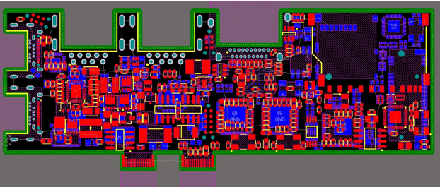
As electronic devices become smaller and more powerful, the demand for Fine Pitch PCBs—boards designed for components with extremely small pin spacing—has grown significantly. Fine pitch components, such as BGA, QFN, and CSP packages, require precise PCB design and manufacturing to ensure electrical connectivity, signal integrity, and long-term reliability.
Design Considerations
-
High-Density Layouts:
Fine pitch PCBs are often used in compact devices where space is limited. Designers must optimize trace routing, via placement, and component orientation to avoid shorts and maintain signal integrity, while maximizing the use of board real estate. -
Controlled Impedance and Signal Integrity:
High-speed signals on fine pitch PCBs are sensitive to parasitic capacitance and crosstalk. Differential pair routing, impedance control, and proper layer stack-up design are essential to minimize signal degradation. -
Via and Pad Optimization:
Microvias, blind vias, and carefully dimensioned pads ensure reliable connectivity for densely packed components. Staggered or buried via strategies may be used to accommodate routing without interfering with other layers. -
Thermal and Mechanical Considerations:
Fine pitch components generate heat and require precise thermal management. Copper pours, thermal vias, and heat-spreading planes help dissipate heat effectively, while proper material selection prevents warping and delamination during assembly and reflow.
Manufacturing Challenges
Producing fine pitch PCBs requires advanced fabrication techniques:
-
High-Precision Etching: Accurate trace widths and spacing are critical to prevent shorts and opens.
-
Sequential Lamination: Multiple layers must be laminated with exact alignment to support microvias and maintain planarity.
-
Advanced Solder Mask and Surface Finish: Fine-pitch boards require precise solder mask application and finishes like ENIG or OSP to ensure consistent solderability.
-
Inspection and Process Control: High-resolution AOI, X-ray inspection, and automated handling systems prevent defects in densely populated boards.
KKPCB leverages these advanced manufacturing capabilities to produce high-density fine pitch PCBs with high yield and reliability.
Testing and Quality Assurance
Due to their complexity, fine pitch PCBs undergo rigorous inspection and testing:
-
Electrical Testing: Ensures all fine-pitch pads and traces maintain continuity and correct impedance.
-
X-ray and Cross-Section Inspection: Confirms microvia connectivity and solder joint integrity under dense BGA or CSP packages.
-
Thermal Cycling and Reliability Testing: Verifies performance under repeated heat stress and operational conditions.
-
Functional Testing: Fine pitch PCBs may undergo simulated system-level operation to confirm signal integrity and overall functionality.
Applications of Fine Pitch PCBs
Fine pitch PCBs are widely used in applications where high density and precision are critical:
-
Mobile Devices and Wearables: Supporting compact and high-pin-count ICs.
-
High-Speed Computing and Servers: Ensuring reliable high-frequency signal routing for processors and memory modules.
-
Automotive Electronics: Supporting ECUs, ADAS modules, and high-density sensor boards.
-
Industrial IoT Devices: Enabling compact controllers and communication modules for dense embedded systems.
By integrating advanced design, precise fabrication, and thorough testing, KKPCB delivers fine pitch PCBs that meet the stringent demands of modern high-density electronics, ensuring performance, reliability, and manufacturability.
