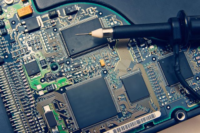
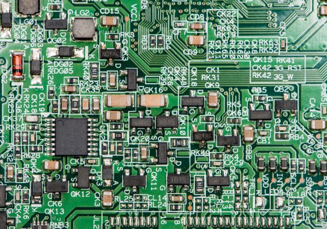
A Fine Pitch PCB is a high-precision printed circuit board designed to support fine pitch IC packages, such as fine-pitch BGA, QFN, CSP, and advanced semiconductor test sockets. As modern electronic devices continue to demand higher integration, smaller form factors, and faster signal speeds, fine pitch PCB technology has become essential for achieving reliable electrical connectivity and stable signal performance.
Fine pitch PCBs are widely used in semiconductor testing, high-speed digital systems, RF modules, automotive electronics, and advanced communication equipment, where accuracy and reliability are critical.
Key Characteristics of Fine Pitch PCB Technology
1. Ultra-Fine Line and Space Capability
Fine pitch PCBs utilize ultra-fine trace width and spacing, enabling precise breakout routing for dense IC pads without compromising electrical performance.
2. High Pin Count Package Support
Advanced ICs often feature hundreds or thousands of pins. Fine pitch PCBs provide reliable fan-out solutions for high pin count packages, ensuring complete signal access.
3. HDI and Microvia Structures
Fine pitch PCBs commonly incorporate HDI technology, including microvias, blind vias, and buried vias, to maximize routing density and improve signal integrity.
4. Controlled Impedance Routing
High-speed and RF applications require strict impedance control. Fine pitch PCB designs ensure consistent impedance for differential pairs and critical signal paths.
5. Multilayer PCB Architecture
Fine pitch PCBs often adopt multilayer stackups to separate signal, power, and ground planes, reducing EMI and improving overall electrical stability.
Applications of Fine Pitch PCBs
Fine pitch PCBs are widely applied in:
-
Semiconductor test PCBs (ATE boards, probe cards, load boards)
-
High pin count IC test boards
-
High-speed digital and mixed-signal electronics
-
RF and wireless communication modules
-
Automotive electronics and ADAS systems
-
Medical and industrial control devices
These applications demand high routing accuracy, reliable interconnections, and stable signal integrity.
Manufacturing Requirements for Fine Pitch PCBs
Producing high-quality fine pitch PCBs requires:
-
Advanced HDI fabrication processes
-
Laser drilling for microvias
-
Precision imaging and etching control
-
Tight registration and alignment tolerance
-
Controlled impedance testing and verification
-
Support for prototype, small batch, and mass production
Strict manufacturing control ensures high yield, repeatable quality, and long-term reliability.
Why Fine Pitch PCB Quality Is Critical
Low-quality fine pitch PCBs can cause:
-
Short circuits or open connections
-
Signal distortion and impedance mismatch
-
Assembly failures during IC placement
-
Reduced test accuracy and product reliability
A professionally manufactured Fine Pitch PCB ensures stable electrical performance, high assembly yield, and dependable operation in demanding applications.
Conclusion
The Fine Pitch PCB is a cornerstone technology for modern electronics requiring high pin count support, compact layouts, and precise signal control. By leveraging HDI technology, microvia structures, fine line routing, and multilayer design, fine pitch PCBs deliver reliable, high-performance solutions for advanced electronic and semiconductor systems.
Choosing an experienced fine pitch PCB manufacturer enables faster development cycles, improved product yield, and long-term system reliability.
