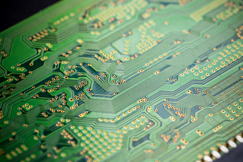
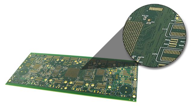
A Fine Line PCB is a printed circuit board that features extremely narrow traces and spacing, typically in the range of 2–4 mils (50–100 μm), allowing engineers to fit more functionality into a smaller board area. Fine line technology is critical for high-density, high-speed digital, RF, and precision analog circuits, where both space optimization and signal integrity are essential.
Fine line PCBs are widely used in:
-
High-speed communication devices
-
Advanced computing and server boards
-
Aerospace and defense electronics
-
Compact consumer electronics like smartphones and wearables
Design Challenges
Fine line PCB design introduces several technical challenges:
-
Trace and Spacing Limitations: Narrow traces increase the risk of open circuits and reduce current-carrying capacity.
-
Signal Integrity Issues: High-speed signals require controlled impedance; narrow traces amplify the effect of parasitic capacitance and inductance.
-
Thermal Management: Fine traces generate more heat per unit area, creating potential hotspots in high-power sections.
-
Manufacturing Tolerances: Slight deviations in etching or lamination can compromise board reliability.
-
Reliability under Environmental Stress: Fine lines are more susceptible to delamination, cracking, or shorting under thermal or mechanical stress.
Engineering Solutions
Engineers address these challenges with a combination of design strategies and process controls:
-
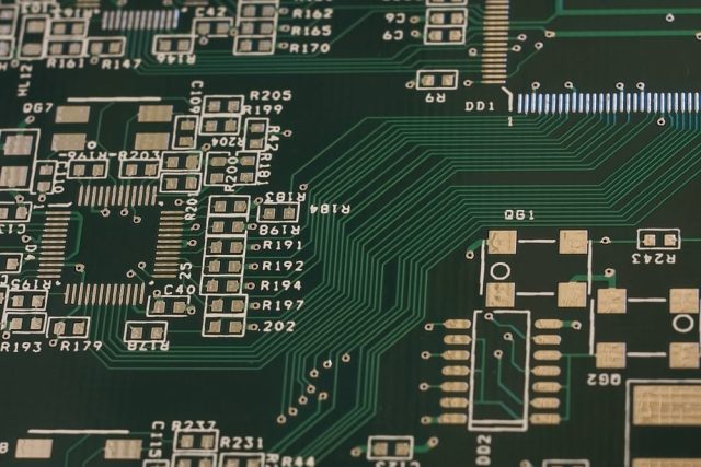
Advanced Layout Techniques: Optimized trace routing, differential pair design, and via placement reduce crosstalk and maintain signal integrity.
-
Impedance Control: Careful calculation of trace width, dielectric constant, and layer stack-up ensures consistent impedance for high-speed signals.
-
Copper Weight and Thickness Optimization: Selecting appropriate copper thickness balances current capacity and manufacturability.
-
Thermal Considerations: Thermal vias, heat-spreading copper planes, and localized metal areas dissipate heat from high-density sections.
-
Design for Manufacturability (DFM): Collaboration with PCB fabricators ensures tolerances for etching, lamination, and plating meet the fine line specifications.
Material & Fabrication Considerations
Producing fine line PCBs requires advanced materials and fabrication techniques:
-
Low-Loss Laminates: High-frequency laminates reduce dielectric loss and preserve signal quality in RF and high-speed digital circuits.
-
High-Resolution Photolithography: Enables precise etching of sub-4 mil traces with minimal deviations.
-
Surface Finishes: ENIG, immersion silver, or hard gold finishes improve solderability and protect ultra-fine traces.
-
Quality Assurance:
-
Automated Optical Inspection (AOI) detects micro-defects in traces and vias
-
X-ray inspection ensures multilayer registration
-
Thermal cycling tests confirm mechanical and electrical stability under operational stress
-
KKPCB leverages these methods to deliver reliable, high-density fine line PCBs capable of handling modern electronic demands.
Applications & Case Highlights
Fine line PCBs are essential in applications requiring compact size and high signal fidelity:
-
Smartphones and Wearables: Dense circuits for high-speed processing in limited space
-
High-Speed Networking: Server and router boards requiring multi-gigabit signal transmission
-
Aerospace & Defense Electronics: Lightweight, high-density boards for avionics and radar systems
-
Medical Devices: Miniaturized boards for imaging, monitoring, and diagnostic equipment
In practice, fine line PCBs enable engineers to maximize functionality while preserving signal integrity, meeting the rigorous performance and reliability standards of advanced electronics.
