What Is a Fine Line PCB?
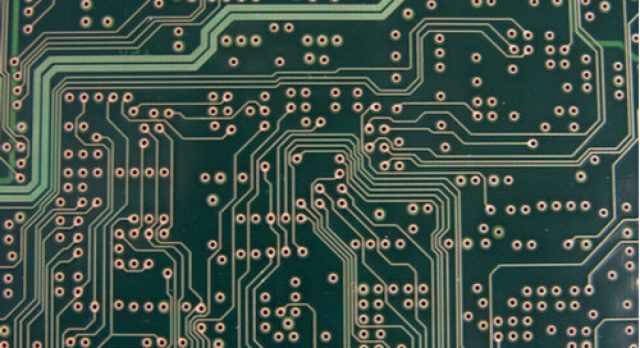
A Fine Line PCB refers to a printed circuit board manufactured with extremely narrow trace widths and spacing. Compared with standard PCB designs, fine line technology enables higher routing density within limited board space.
Fine line PCBs are essential for modern electronic devices where compact size, high functionality, and complex signal routing are required.
What Defines “Fine Line”?
Fine line capability is typically measured by trace width and spacing:
-
Standard PCB: ≥ 4/4 mil
-
Advanced PCB: 3/3 mil
-
Fine Line PCB: 2/2 mil or below
-
Ultra-fine structures: 1.5/1.5 mil or smaller
The smaller the line width and spacing, the higher the circuit density that can be achieved.
Why Fine Line Technology Is Important
As electronic components continue to shrink and pin counts increase, routing space becomes limited. Fine line PCB enables:
-
Higher component density
-
Improved signal routing flexibility
-
Reduced board size
-
Increased layer utilization efficiency
This is especially important for high-speed digital, mobile, and advanced computing systems.
Key Manufacturing Technologies
Producing fine line PCB requires advanced fabrication control, including:
1. High-Resolution Imaging
Precise photoresist imaging ensures accurate trace definition and minimal line deviation.
2. Advanced Etching Control
Tight etching process control prevents over-etching or undercutting, maintaining consistent conductor width.
3. Laser Direct Imaging (LDI)
LDI improves pattern accuracy and alignment, especially in HDI structures.
4. Precise Copper Thickness Management
Copper weight must be optimized to maintain fine geometry without affecting electrical performance.
Design Considerations
When designing a fine line PCB, engineers must consider:
-
Impedance control impact
-
Current carrying capability
-
Copper thickness selection
-
Manufacturability limits
-
Yield considerations
Narrow traces may limit current capacity, so power and signal routing must be carefully separated.
Applications of Fine Line PCB
Fine line PCBs are widely used in:
-
HDI smartphones and tablets
-
High-speed computing modules
-
AI accelerator boards
-
Networking equipment
-
Automotive electronics
-
Medical devices
-
Wearable electronics
As devices become more compact and powerful, fine line technology becomes increasingly necessary.
Fine Line PCB vs Standard PCB
| Feature | Standard PCB | Fine Line PCB |
|---|---|---|
| Trace Width | ≥4 mil | ≤2 mil |
| Circuit Density | Moderate | High |
| Manufacturing Complexity | Standard | Advanced |
| Board Size Optimization | Limited | Improved |
| Cost | Lower | Higher |
Fine line PCB enables more routing in limited space but requires tighter process control.
Conclusion
Fine Line PCB technology plays a critical role in enabling compact, high-density electronic systems. By supporting extremely narrow trace widths and spacing, it allows designers to increase functionality without expanding board size.
For advanced electronics requiring miniaturization and high routing density, fine line PCB provides a precise and reliable manufacturing solution.
