Ensuring High-Performance PCB Fabrication
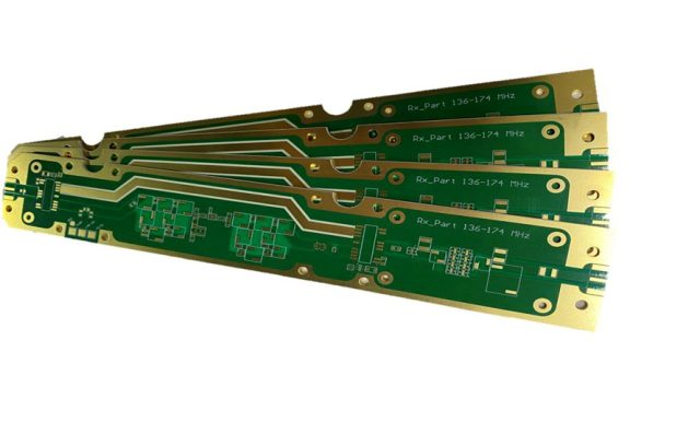
RO4360G2 high-frequency laminates are engineered for RF, microwave, and high-speed PCB applications, offering excellent dielectric stability, low loss, and high thermal reliability. To maximize their performance, precise fabrication guidelines must be followed during PCB manufacturing, layer stack-up, and assembly.
Proper handling and design considerations are essential for maintaining signal integrity, impedance control, and mechanical reliability in demanding environments such as aerospace, telecommunications, and industrial RF systems.
Material Overview: RO4360G2 Laminates
RO4360G2 is a high-frequency laminate designed for:
- Microwave circuits
- Antenna modules
- RF/microwave communication devices
- High-reliability industrial applications
Key Material Properties
- Dielectric constant (Dk): 6.15 @ 10 GHz
- Dissipation factor (Df): 0.0037 @ 10 GHz
- Low thermal expansion coefficient
- High thermal conductivity
- Excellent mechanical stability
These properties make RO4360G2 ideal for high-frequency, high-power, and high-reliability PCB designs.
Design Guidelines for RO4360G2
1. Controlled Impedance Design
- Maintain precise trace width and spacing
- Use appropriate stack-up configurations to minimize parasitic effects
- Design ground planes to reduce EMI and ensure signal integrity
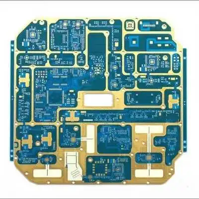
2. Multilayer Stack-Up Recommendations
- Keep signal layers close to reference planes
- Use thick copper planes for power distribution and thermal management
- Limit layer count to balance manufacturability and RF performance
3. Thermal Considerations
- RO4360G2 supports high-temperature operation, but controlled lamination is essential
- Ensure sufficient heat dissipation for high-power RF circuits
- Consider thermal vias for effective heat transfer
Fabrication Best Practices
1. Drilling and Plating
- Use sharp drill bits to avoid delamination in PTFE-based laminates
- Maintain tight tolerance for via diameters
- Implement proper plating thickness for signal and power vias
2. Lamination Process
- Follow controlled temperature and pressure profiles
- Prevent warpage and maintain flatness of multilayer boards
- Use proper bonding prepreg materials compatible with RO4360G2
3. Solder Mask and Surface Finish
- Select high-temperature solder mask to match thermal profile
- Use ENIG or OSP finishes for optimal wirebonding and soldering reliability
- Avoid excessive heat to prevent delamination or pad lift
4. Component Assembly
- Use low-loss solder paste for high-frequency components
- Maintain controlled reflow profiles to avoid material stress
- Implement proper placement for RF-critical components
Testing and Quality Assurance
- Impedance verification for controlled signal traces
- Insertion loss testing for high-frequency circuits
- X-ray and AOI inspections for multilayer boards
- Thermal cycling and mechanical stress tests for reliability
Applications of RO4360G2 Laminates
RO4360G2 is ideal for:
- High-power RF amplifiers
- Microwave and radar modules
- Satellite and aerospace electronics
- 5G communication infrastructure
- Industrial high-frequency sensor systems
Its high Dk and thermal stability make it suitable for high-frequency circuits that demand low loss and robust mechanical performance.
Conclusion: Optimizing High-Frequency PCB Fabrication
By following proper fabrication guidelines, including controlled impedance design, thermal management, and assembly best practices, engineers can ensure RO4360G2 high-frequency laminates achieve their full potential. These laminates deliver reliable RF performance, low insertion loss, and mechanical stability for demanding applications in aerospace, telecommunications, and industrial sectors.
