5G router PCB platforms operate under multi-band RF loads, high-density routing, and continuous thermal cycling in compact CPE enclosures. Achieving stable RF efficiency requires a stackup engineered around low-loss materials, controlled dielectric stability, and carefully optimized thermal paths. This article analyzes how engineered 5G router PCB stackups improve RF efficiency, insertion-loss performance, and long-term thermal reliability for Wi-Fi 6/7 + Sub-6G + mmWave hybrid routers.
Core Engineering Challenges
5G router PCB systems encounter several tightly coupled engineering constraints.
RF insertion loss grows rapidly with frequency, especially above 3–6 GHz. Dielectric consistency becomes critical to prevent mismatch drift across multi-band pathways. Meanwhile, thermal density in high-power PA (power amplifier) zones stresses the laminate stack, risking via fatigue, copper migration, and Dk wandering.
The engineering objective is to build a low-loss, RF-stable, thermally robust PCB architecture capable of supporting complex routing for MIMO, beamforming, and multi-antenna isolation.
Material Science & Dielectric Performance
Low-loss laminates—such as Megtron 7, RO4350B, or RF-focused hydrocarbon-ceramic blends—form the foundation of high-performance 5G router PCB stackups. These materials reduce insertion loss, stabilize Dk/Df, and suppress dielectric-induced phase shift.
Combining them with thermally conductive prepregs or ceramics enhances heat spreading in PA regions.
Material Parameter Table
| Parameter | Low-Loss RF Laminate | Standard FR-4 |
|---|---|---|
| Dielectric Constant (10 GHz) | 3.0–3.5 | 4.2–4.6 |
| Dissipation Factor | 0.002–0.004 | 0.015–0.020 |
| Thermal Conductivity | 0.5–1.0 W/m·K | 0.25 W/m·K |
| RF Insertion Loss (6 GHz) | Low | High |
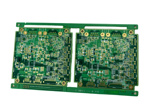
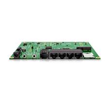
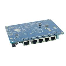
KKPCB Case Study — 5G Router PCB (CPE System)
Industry Application
High-power 5G router systems including indoor CPE, industrial gateways, and outdoor fixed wireless terminals.
Customer Background
A networking OEM needed a multi-band 5G router PCB supporting 8× MIMO operation while achieving stable PA thermal dissipation under 24/7 load.
Engineering Problems
• High insertion loss at 5–7 GHz channels
• Excessive heat rise near PA modules
• Dk drift causing mismatch between RF layers and antenna feedlines
KKPCB Solution
We engineered a hybrid stackup using low-loss RF cores + thermally enhanced layers. HFSS simulations guided microstrip width tuning, while ADS validated PA matching networks. Thermal FEM verified hotspot suppression.
Measurement Results
| Metric | Before | After KKPCB Optimization |
|---|---|---|
| Insertion Loss @ 6 GHz | -1.45 dB | -0.76 dB |
| PA Temperature Rise | +28°C | +14°C |
| Dk Stability (Across Layer) | ±0.09 | ±0.02 |
Stackup Design & RF Implementation
The PCB stack integrated:
• Dual RF core layers for Sub-6G and Wi-Fi 7
• Microstrip & grounded CPW routing for isolation
• Buried-via RF transitions to minimize stub resonance
• Heat-spreading ceramic-filled dielectric under PA zones
RF sensitivity regions were modeled in HFSS, while TDR verified impedance on 85–95 Ω differential lines.
Example 5G Router PCB Stackup
| Layer | Function |
|---|---|
| L1 | Antenna, RF microstrip |
| L2 | RF ground plane |
| L3–L4 | Low-loss RF core |
| L5 | Digital control & high-speed lanes |
| L6 | Ground & shielding |
Environmental & Reliability Validation
5G router systems operate under constant thermal loading, so reliability validation included:
Reliability Tests
| Test | Result |
|---|---|
| Thermal Cycling -40°C to +125°C | Pass (No via fatigue) |
| Humidity 85°C/85% 240 hrs | Pass |
| Vibration | Pass |
| Reflow (3× at 260°C) | Pass |
Engineering Summary & Contact
Advanced 5G router PCB stackups with low-loss materials and thermally enhanced layers significantly boost RF efficiency, lower insertion loss, and stabilize dielectric behavior under long-term operation. KKPCB provides engineered stackups optimized for high-frequency routing, MIMO isolation, and PA thermal performance.
