Next-generation 112G/224G SerDes channels push FR-4 far beyond its electrical limits. As data center switching, AI computing, and PCIe-6/7 architectures scale upward, loss tangent, copper roughness, and impedance drift become critical bottlenecks. Megtron 7 PCB laminates—Df 0.0012 class, highly stable Dk, and low copper-permittivity interaction—provide an electrically clean foundation for long-reach PAM4 channels.
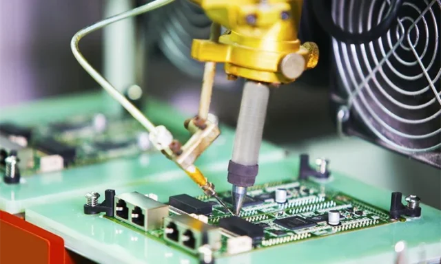
KKPCB integrates Megtron 7 PCB stackups with controlled glass styles, ultra-smooth copper, and precision lamination to minimize insertion loss and maintain channel linearity across long backplane runs.
Engineering Challenges for 112G/224G Channels
High-speed systems operating at 56–112 GHz Nyquist frequencies face a cluster of signal-integrity obstacles:
• Loss accumulation caused by copper roughness and dielectric dissipation
• Crosstalk coupling due to dense differential-pair clustering
• Impedance drift triggered by resin-glass variation in multilayer stacks
• PAM4 eye collapse from reflections, skew, and via stubs
• Thermal rise in AI racks causing Dk shift in subpar materials
Megtron 7 PCB materials address these high-speed limits directly with low-loss, stable dielectric behavior ideal for PAM4 modulation.
Material Science — Why Megtron 7 PCB Excels
Megtron 7 PCB laminates deliver:
• Ultra-low Df (0.0012–0.0020 range) → reduced insertion loss for 112G/224G
• Tightly controlled Dk (3.3 class) → predictable impedance and low skew
• Low CTE → dimensional stability during reflow
• Low dielectric anisotropy → consistent channel performance across layers
• Reduced glass weave effect → minimized differential skew at long distances
The material’s behavior at ultra-high frequencies makes Megtron 7 PCB one of the few reliable choices for next-generation high-speed infrastructure.
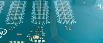
KKPCB Case Study — 224G Switch Backplane PCB
Problem:
A customer’s 224G PAM4 switch backplane using a Megtron-6 equivalent material exhibited excessive IL loss >0.7 dB/in at 26 GHz and unstable impedance across heavy copper zones.
KKPCB Megtron 7 Implementation:
• Optimized Megtron 7 PCB stackup with symmetrical glass styles
• Very-low-profile copper (VLP, Ra <0.7 µm)
• Backdrilled via design reducing stub length below 6 mil
• Tight lamination tolerance ±8 µm
• Distributed via-to-via isolation for deep-reach channels
Results After KKPCB Engineering:
| Parameter | Achieved |
|---|---|
| IL @26 GHz | 0.46 dB/in |
| Crosstalk | –17.5 dB |
| Intra-pair skew | <0.6 ps |
| Return loss | –19.2 dB |
This achieved full margin for 224G PAM4 compliance with additional channel headroom.
Simulation & Stackup Engineering
Using HFSS, ADS, and Sigrity:
• Channel IL flattened by 22% after copper-roughness optimization
• Impedance window held at ±5% across a 24-layer Megtron 7 PCB
• Backdrill depth optimized to avoid 20–30 GHz resonance bands
• Thermal FEM confirmed dielectric stability under 90°C sustained operation
Validation & Reliability Testing
• Thermal cycling –40°C ↔ 110°C: no Dk shift beyond 0.02
• Multi-reflow 260°C × 6 cycles: no warpage
• Vibration testing: no micro-fractures in high-density via arrays
Engineering Summary
Megtron 7 PCB technology enables ultra-low-loss, stable routing for advanced 112G/224G SerDes systems. Through controlled copper roughness, careful glass-style selection, and precise lamination, KKPCB delivers robust, margin-rich high-speed channels suitable for next-generation data center equipment.
