Low Dissipation Factor PCB Engineering for High-Frequency, High-Power, and Low-Loss Electronic Platforms
A Low Dissipation Factor PCB is the backbone of modern high-frequency hardware, designed to minimize dielectric loss, reduce signal attenuation, and maintain stable RF performance across extreme bandwidths. As systems scale into mmWave, sub-THz, and multi-gigabit domains, the dissipation factor (Df) becomes a defining parameter—almost the DNA of high-performance circuit behavior. A low-Df substrate ensures that every transmitted signal maintains maximum amplitude, phase accuracy, and spectral purity.
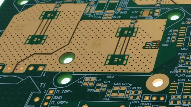
The advantage of a Low Dissipation Factor PCB becomes most visible in RF front-ends, phased-array radar platforms, satellite transceivers, V2X modules, and millimeter-wave imaging systems. In these environments, even small increases in Df generate excessive insertion loss, degrade Q-factors, and complicate impedance tuning. Using engineered low-Df materials such as PTFE composites, ceramic-filled laminates, or ultra-low-loss hydrocarbon blends, designers can preserve high-frequency signal integrity while enabling dense routing and compact multi-layer stackups.
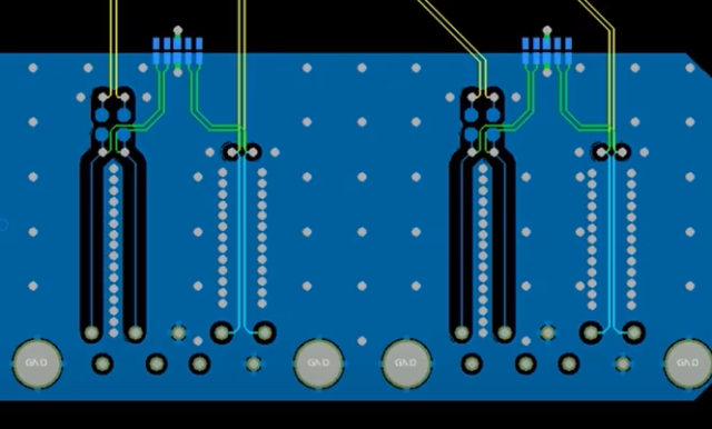
From a manufacturing perspective, a Low Dissipation Factor PCB demands strict process control—lamination pressure stability, copper surface treatment, and low-profile foil selection all influence final dielectric performance. High-frequency engineers often pair low-Df cores with smooth rolled-annealed copper to optimize conductor loss, while maintaining consistent dielectric constants (Dk) across the entire operating environment. This pairing results in reduced propagation delay variation, improved phase matching, and significantly lower insertion loss across 5G bands, Ku-band, Ka-band, and X-band systems.
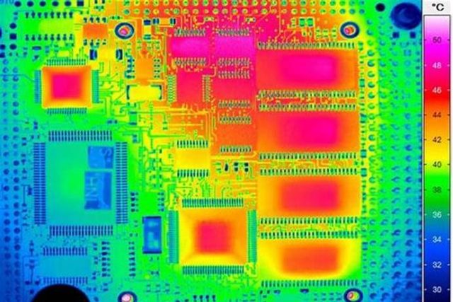
As power levels rise in satellite uplinks, radar transmitters, and high-Q resonant filters, the thermal behavior of a Low Dissipation Factor PCB becomes equally important. Lower dielectric loss translates into lower heat generation, which guarantees reliability, suppresses drift, and enhances component lifetime. Systems that require long-term frequency stability—navigation modules, aerospace communication systems, precision timing blocks—benefit heavily from the predictable thermal response of a low-Df laminate.
For high-speed digital applications, a Low Dissipation Factor PCB is the difference between maintaining eye-diagram clarity or losing the battle to crosstalk and jitter. With the rise of PCIe Gen5/Gen6, 64-Gbps SerDes, and accelerated AI computing fabrics, PCB materials must preserve signal integrity across shrinking rise times and tighter impedance windows. Low-Df materials give designers space to push routing density, integrate differential pairs more tightly, and support ultra-fast data transmission without compromising SNR.
In short, a Low Dissipation Factor PCB is not merely a materials choice. It is a system-level strategy for building RF, microwave, mmWave, and high-speed digital platforms that require low loss, stable phase behavior, excellent thermal reliability, and long-term performance stability. As communication systems, radar modules, satellite payloads, and high-speed computing continue pushing toward higher frequencies and tighter tolerances, low-Df PCB technology will remain a critical enabler of next-generation electronic innovations—balancing electrical performance with manufacturability in a way few other technologies can match.
