1. Engineering Context
As electronic systems push into higher frequencies—5G, mmWave sensing, radar, satellite communication, and precision instrumentation—the dissipation factor (Df) of PCB materials has become a primary performance determinant.
A Low Dissipation Factor PCB minimizes dielectric loss, preserves signal integrity, and ensures stable operation at frequencies where traditional FR-4 rapidly degrades.
Low Df PCBs bridge the gap between material science and high-speed electronics, enabling engineers to design more efficient, accurate, and reliable RF systems.
2. What Is Dissipation Factor (Df)?
The dissipation factor, often written as Df or tan δ, represents how much signal energy is lost as heat while traveling through the dielectric material.
Lower Df = Lower Signal Loss = Better High-Frequency Performance
Typical material comparison:
-
Standard FR-4: Df ≈ 0.015–0.020
-
Low-Loss FR-4: Df ≈ 0.008–0.010
-
High-End Low Df Laminates (Rogers/Megtron): Df ≈ 0.001–0.004
At GHz frequencies, even small differences in Df dramatically affect system performance.
3. Why Low Dissipation Factor PCBs Matter
A. High-Frequency Signal Integrity
Low Df materials preserve amplitude, reduce jitter, and minimize eye-diagram closure.
Ideal for:
-
RF transceivers
-
5G FR2 bands
-
High-resolution radar
-
High-speed digital interfaces (10–112+ Gbps)
B. Reduced Insertion Loss
Lower dielectric loss leads to longer trace routing, reduced need for repeaters, and improved link margin.
C. Improved Phase Stability
Critical for:
-
phased-array antennas
-
beamforming modules
-
precision timing systems
D. Lower Heat Generation
Less dielectric heating increases performance stability and material reliability.
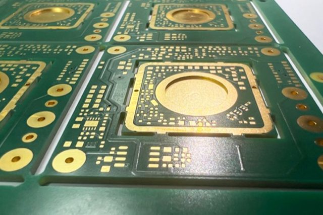
4. PCB Materials for Low Dissipation Factor Applications
High-Performance Low Df Laminates Commonly Used in KKPCB Projects
| Material | Typical Df | Applications |
|---|---|---|
| Rogers RO4350B | 0.0037 | 5G, radar, precision RF |
| Rogers RO4003C | 0.0027 | RF modules, base stations |
| Megtron 6 | 0.002–0.004 | high-speed digital, SerDes |
| Taconic RF-35 | 0.0018 | microwave circuits |
| PTFE Laminates | 0.0009–0.0020 | satellite, aerospace |
These materials maintain performance beyond 10–40 GHz, where FR-4 becomes unusable.
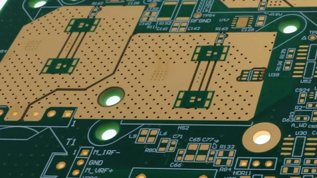
5. Stackup Engineering for Low Df PCBs
A high-performance Low Dissipation Factor PCB requires optimized RF stackup:
A. Precise Dielectric Thickness Control
Thin, consistent layers minimize impedance variation and reduce loss.
B. Copper Roughness Management
Smooth copper foils (VLP/ULP) reduce conductor losses at mmWave frequencies.
C. Grounded Reference Structures
Microstrip and stripline geometries benefit from tightly coupled ground layers.
D. Mixed-Laminate Hybrid Stackups
Combining low Df materials with FR-4 reduces cost without compromising high-frequency sections.
KKPCB engineers frequently design hybrid low-loss stackups for 5G and radar systems.
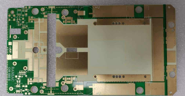
6. Typical Applications of Low Dissipation Factor PCBs
• 5G NR & mmWave Communication
Stable PCB performance up to 40 GHz for base stations, UE modules, and RF front-ends.
• Automotive Radar (24 / 77 / 79 GHz)
Critical for ADAS, long-range radar, and autonomous vehicles.
• Satellite Communication & GNSS
Low loss ensures clearer reception and improved link reliability.
• High-Speed Computing
Essential for 56G/112G SerDes, PCIe 5.0/6.0, and advanced networking.
• Precision Instrumentation
Low phase drift and noise stability for measurement-grade electronics.
7. Reliability Considerations
Low Df PCBs must also withstand:
-
wide temperature swings
-
vibration (aerospace, automotive)
-
humidity and oxidation
-
long-term RF heating
KKPCB applies:
-
IPC-6012 Class 3 standards
-
thermal aging
-
RF stress testing
-
dielectric breakdown assessment
ensuring long-term stability even under continuous GHz-level operation.
8. Engineering Summary
A Low Dissipation Factor PCB is fundamental to any system requiring high-frequency stability, minimal loss, and uncompromised RF precision. Through advanced material selection, optimized copper structures, and engineered stackups, designers can dramatically improve signal integrity, reduce insertion loss, and increase system reliability.
KKPCB offers complete engineering and manufacturing solutions for Low Df PCBs, including hybrid stackups, RF/microwave layout, mmWave structures, and IPC Class 3 reliability assurance.
