Differential Pair PCB: Design Guidelines for High-Speed Signal Integrity
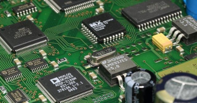
In modern high-speed digital systems, Differential Pair PCB routing has become a fundamental design technique for maintaining signal integrity and reducing electromagnetic interference. Interfaces such as USB, HDMI, PCIe, Ethernet, and high-speed SerDes rely heavily on differential signaling to achieve reliable high-speed data transmission.
A well-designed differential pair PCB layout ensures balanced signal propagation, controlled impedance, and minimal noise coupling. This article explores the core design principles, routing strategies, and manufacturing considerations for differential pair PCB design in high-speed electronic systems.
What Is a Differential Pair PCB?
A Differential Pair PCB refers to a printed circuit board layout where two traces carry equal and opposite signals. Instead of referencing a single-ended signal to ground, differential signaling transmits data through the voltage difference between two traces.
Key characteristics of differential pair signals include:
-
Equal and opposite current flow
-
Reduced susceptibility to external noise
-
Lower electromagnetic radiation
-
Improved signal integrity at high data rates
Because of these advantages, differential pair routing is widely used in high-speed PCB design and signal integrity engineering.
Advantages of Differential Pair PCB Design
1. Improved Noise Immunity
Differential signals reject common-mode noise because both traces experience the same interference, which cancels out at the receiver.
2. Reduced Electromagnetic Interference (EMI)
Balanced current flow minimizes radiation, making differential pair PCB routing suitable for high-speed communication interfaces.
3. Higher Data Transmission Speed
Differential signaling supports faster data rates compared to traditional single-ended signaling methods.
4. Better Signal Integrity
With controlled impedance and matched trace lengths, differential pair PCBs maintain stable signal transmission across long routing distances.
Key Differential Pair PCB Design Guidelines
1. Controlled Differential Impedance
Differential pairs require a specific impedance value, commonly 100Ω differential impedance for high-speed digital interfaces. This impedance depends on:
-
Trace width
-
Trace spacing
-
Dielectric thickness
-
PCB material properties
Accurate impedance control ensures minimal signal reflections and optimal transmission.
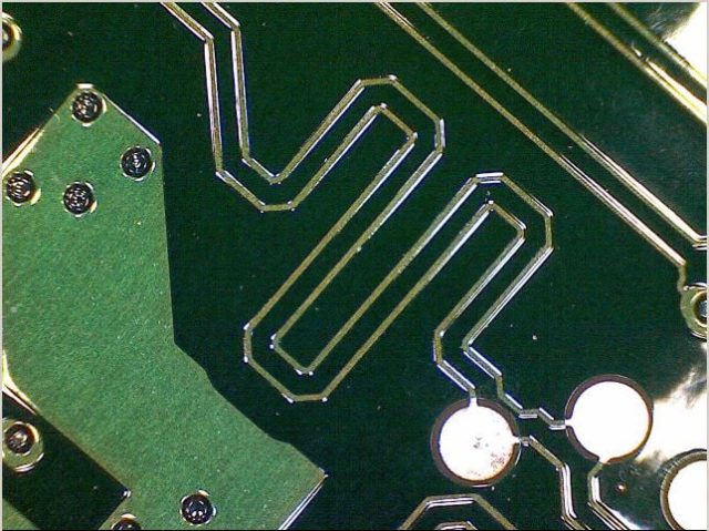
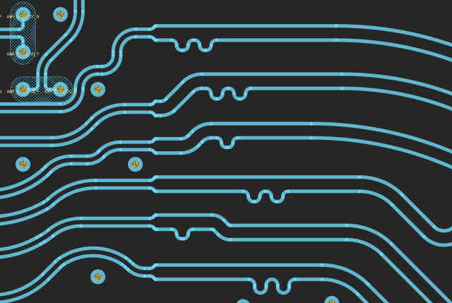
2. Length Matching
Both traces in a differential pair must have nearly identical lengths to prevent timing skew. Even small differences can degrade signal integrity in high-speed systems.
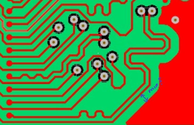
3. Consistent Trace Spacing
Maintaining constant spacing between differential traces is critical for impedance stability and balanced signal coupling.
4. Minimal Via Usage
Each via introduces impedance discontinuity. When vias are necessary, both traces should transition layers simultaneously to maintain symmetry.
5. Reference Plane Integrity
Continuous ground planes beneath differential pair traces provide stable return paths and reduce electromagnetic interference.
PCB Stackup Considerations for Differential Pair Routing
A well-designed multilayer PCB stackup is essential for differential signal performance. Designers often place differential pair routing layers adjacent to solid ground planes to achieve consistent impedance control.
Typical differential pair structures include:
-
Microstrip differential pairs
-
Stripline differential pairs
-
Coplanar differential pairs with ground
These configurations help optimize signal integrity and reduce crosstalk in high-speed PCB layouts.
Applications of Differential Pair PCB
Differential pair routing is essential in many high-speed communication systems, including:
-
USB and USB-C interfaces
-
HDMI and DisplayPort connections
-
PCIe high-speed interconnects
-
Ethernet networking equipment
-
DDR memory interfaces
-
High-speed data center hardware
In these systems, differential pair PCB design enables reliable data transmission at gigabit and multi-gigabit speeds.
Manufacturing Considerations
Manufacturing tolerance plays a significant role in differential impedance accuracy. PCB manufacturers must control:
-
Trace width precision
-
Dielectric thickness consistency
-
Copper plating variation
-
Etching tolerances
Close collaboration between PCB designers and manufacturers ensures that the final board meets the required differential impedance specifications.
Conclusion
A properly designed Differential Pair PCB is essential for high-speed electronic systems. By implementing controlled impedance routing, precise length matching, consistent spacing, and optimized multilayer stackups, engineers can achieve excellent signal integrity and reliable high-speed data transmission.
As data rates continue to increase in modern electronics, differential pair PCB design will remain a key technique for maintaining performance and minimizing signal degradation.
