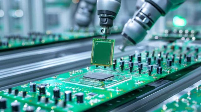
Automated Test Equipment (ATE) systems place some of the most demanding electrical and mechanical requirements on PCB design. An Electrical Requirements in must simultaneously support high-speed digital interfaces, precision analog measurement paths, high pin-count connectivity, and long-term operational stability under continuous duty cycles.
Unlike consumer or general industrial electronics, ATE PCBs function as measurement instruments, not just signal carriers. Any degradation in signal integrity, impedance control, or thermal stability directly impacts test accuracy and yield.
Electrical Requirements in ATE PCB
ATE platforms typically integrate multiple functional domains on a single PCB, including digital pattern generation, high-speed data acquisition, analog front-end conditioning, and power regulation. This mixed-domain environment makes signal isolation and reference control a primary design challenge.
Key electrical design goals for Automated Test Equipment PCBs include:
-
Tight controlled impedance for high-speed digital buses
-
Low-noise analog routing for precision measurement channels
-
Stable reference planes to maintain timing and phase accuracy
-
Minimal crosstalk between adjacent high-density signal paths
Achieving these goals requires careful stackup planning and disciplined routing rules rather than post-layout mitigation.
Stackup Architecture and Material Selection
The PCB stackup is the foundation of ATE electrical performance. Automated Test Equipment PCBs often use high-layer-count stackups to segregate functional domains and maintain predictable impedance environments.
Engineering-driven stackup strategies typically involve:
-
Dedicated ground reference layers for each high-speed signal layer
-
Symmetrical lamination to reduce warpage in large-format boards
-
Low-loss dielectric materials to preserve edge rates and timing margins
-
Controlled dielectric thickness to meet tight impedance tolerances
Material stability over temperature and time is especially critical, as ATE systems are expected to operate continuously with minimal recalibration.
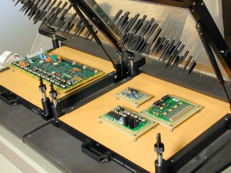
High-Density Interconnect and Via Strategy
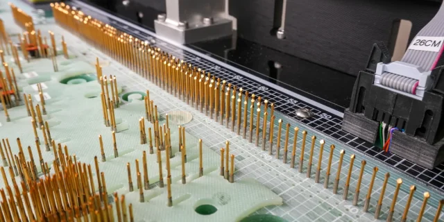
ATE PCBs frequently interface with probe cards, load boards, sockets, and backplanes, resulting in extreme connector density and via congestion. Poor via design introduces stubs, reflections, and skew that directly affect measurement repeatability.
Common engineering practices include:
-
Blind and buried vias to reduce stub length
-
Backdrilling for high-speed vertical transitions
-
Consistent via structures across critical signal paths
-
Optimized antipad sizing to control impedance discontinuities
In Automated Test Equipment PCBs, via structures are treated as transmission line elements, not parasitics to be ignored.
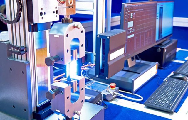
Thermal Stability and Mechanical Reliability
ATE systems generate localized heat from drivers, receivers, and power devices while operating in controlled but continuous environments. PCB thermal behavior must remain stable to avoid electrical drift.
Thermal and mechanical design considerations include:
-
Copper balancing to prevent board deformation
-
High-Tg materials to maintain mechanical integrity
-
Controlled CTE behavior for connector and socket alignment
-
Power plane design that supports both current delivery and heat spreading
Mechanical reliability is particularly important due to repeated insertion cycles and long service lifetimes.
Manufacturing Consistency and Test Repeatability
From a manufacturing perspective, an Automated Test Equipment PCB must be highly repeatable. Small process variations can introduce measurable differences between test channels, affecting calibration and correlation.
Engineering-grade fabrication controls focus on:
-
Tight impedance tolerance management
-
Consistent copper plating thickness
-
Fine-line etching accuracy for dense routing
-
Electrical testing aligned with ATE functional requirements
ATE PCB fabrication is less about yield maximization and more about performance uniformity across boards and production lots.
Engineering Perspective
An Automated Test Equipment PCB is a critical component of the test system’s accuracy, stability, and credibility. Its design requires a system-level understanding of signal behavior, materials science, and manufacturing process control.
By applying controlled impedance stackups, robust via strategies, and production-grade fabrication discipline, KKPCB supports ATE designers in building PCBs that perform as reliable measurement platforms—not just interconnect substrates.
