What Is a Controlled Impedance PCB?
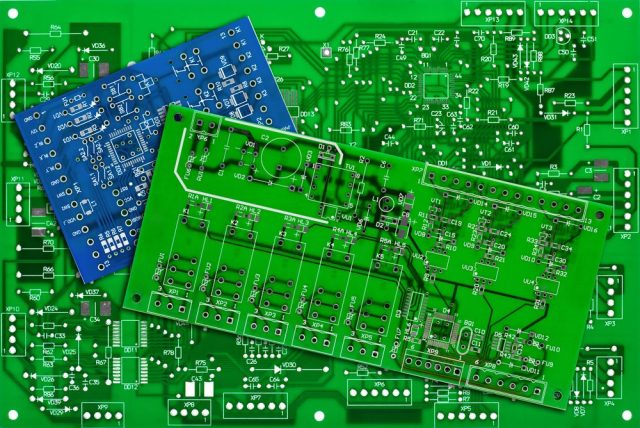
A Controlled Impedance PCB is a printed circuit board designed to maintain a specified electrical impedance value along signal traces. Controlled impedance is critical for maintaining signal quality in high-speed, high-frequency, and RF electronic systems.
In modern electronic devices, high data rate signals require precise impedance matching to prevent signal reflection, distortion, and transmission loss. Controlled impedance PCB technology ensures consistent electrical performance and reliable system operation.
Why Controlled Impedance PCB Is Important
Controlled Impedance PCB design plays a crucial role in modern circuit performance. Improper impedance matching can lead to signal degradation, electromagnetic interference, and system instability.
Key benefits of Controlled Impedance PCB include:
-
Improved signal integrity
-
Reduced signal reflection
-
Enhanced high-speed data transmission
-
Lower electromagnetic interference (EMI)
-
Stable RF signal performance
-
Increased product reliability
As signal frequencies and data rates continue to increase, controlled impedance PCBs have become essential in advanced electronic products.
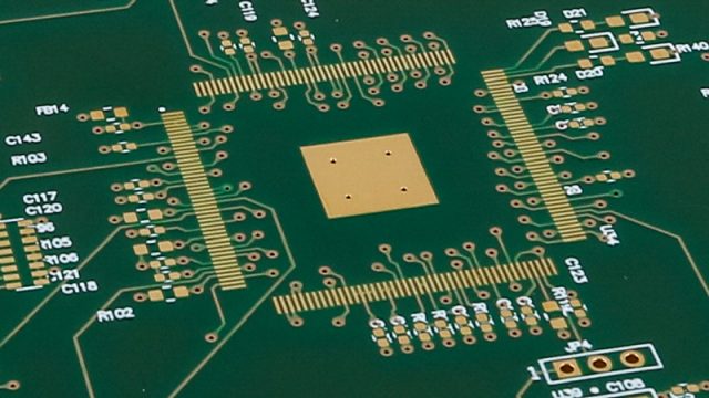
How Controlled Impedance PCB Works
Controlled impedance PCBs maintain target impedance values by controlling several physical parameters, including:
-
Trace width and spacing
-
Dielectric material properties
-
Copper thickness
-
Distance between signal layer and reference plane
-
PCB stack-up structure
By precisely managing these factors, PCB manufacturers can produce boards that meet strict impedance requirements such as 50Ω single-ended or 100Ω differential impedance.
Types of Controlled Impedance Structures
Controlled Impedance PCB designs typically include several transmission line structures:
Microstrip
Signal trace located on an outer PCB layer referenced to an internal ground plane.
Stripline
Signal trace located between two reference planes for improved shielding and reduced EMI.
Differential Pair Routing
Two matched signal traces used for high-speed differential signal transmission.
Each structure is selected based on signal speed, routing requirements, and electromagnetic performance.
Materials Used in Controlled Impedance PCB
Material selection directly affects impedance stability and signal performance. Common materials used in Controlled Impedance PCB fabrication include:
-
High TG FR-4 materials
-
Low loss dielectric laminates
-
Rogers RF materials
-
Megtron high-speed materials
-
Hybrid high-frequency PCB stack-ups
These materials provide stable dielectric constant and low signal loss for high-speed transmission.
Controlled Impedance PCB Manufacturing Process
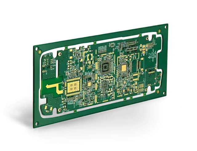
Producing Controlled Impedance PCBs requires advanced manufacturing technology and strict process control, including:
-
Stack-up design verification
-
Impedance simulation and calculation
-
Precision lamination process
-
Controlled etching and copper thickness control
-
Test coupon fabrication for impedance verification
-
Time-domain reflectometer (TDR) testing
Accurate testing ensures the final PCB meets target impedance requirements.
Design Considerations for Controlled Impedance PCB
Successful Controlled Impedance PCB design requires collaboration between design engineers and PCB manufacturers. Important design considerations include:
-
Early stack-up planning
-
Consistent trace routing rules
-
Ground plane continuity
-
Differential pair length matching
-
Avoiding impedance discontinuities
-
Thermal and mechanical stability
Design for manufacturability (DFM) review is essential to ensure production success.
Applications of Controlled Impedance PCB
Controlled Impedance PCBs are widely used in advanced electronic systems such as:
-
High-speed networking and data communication equipment
-
5G infrastructure and wireless communication modules
-
RF and microwave systems
-
AI servers and high-performance computing devices
-
Automotive ADAS and radar systems
-
Aerospace and defense electronics
-
Medical imaging and diagnostic equipment
-
Semiconductor test and evaluation systems
These applications require precise signal transmission and high electrical reliability.
Conclusion
A Controlled Impedance PCB is essential for maintaining signal integrity in high-speed and high-frequency electronic applications. Through precise stack-up design, advanced materials, and strict manufacturing control, impedance controlled PCBs provide stable electrical performance and reliable product functionality.
Partnering with an experienced Controlled Impedance PCB manufacturer ensures accurate impedance verification, consistent fabrication quality, and reliable delivery for complex electronic projects.
