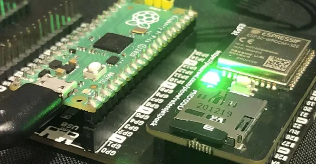
A Controlled Impedance PCB is a critical foundation for modern high-speed digital systems and high-frequency RF applications. As signal rise times shrink and operating frequencies extend into multi-GHz ranges, PCB interconnects must behave as predictable transmission lines rather than simple copper connections. Controlled Impedance PCB design ensures signal integrity, phase stability, and EMI compliance across complex electronic systems.
Understanding Controlled Impedance PCB
A Controlled Impedance PCB is engineered so that signal traces maintain a predefined characteristic impedance—commonly 50Ω single-ended or 90Ω/100Ω differential—within strict tolerances. This impedance is governed by electromagnetic field behavior, not just trace width. Copper geometry, dielectric constant (Dk), dielectric thickness, and reference plane configuration together define impedance performance.
Without controlled impedance, signal reflections, eye-diagram collapse, jitter, and electromagnetic interference become unavoidable in high-speed PCB designs.
Transmission Line Behavior in Controlled Impedance PCB Design
In Controlled Impedance PCB layouts, every high-speed trace must be treated as a transmission line with distributed resistance, inductance, and capacitance. Microstrip, stripline, and coplanar waveguide structures are commonly used to achieve controlled impedance across different PCB layers.
Stripline routing offers superior impedance consistency due to full dielectric enclosure, while microstrip structures simplify fabrication but require tighter control of dielectric thickness and copper roughness. Selecting the correct transmission structure is a core decision in Controlled Impedance PCB engineering.
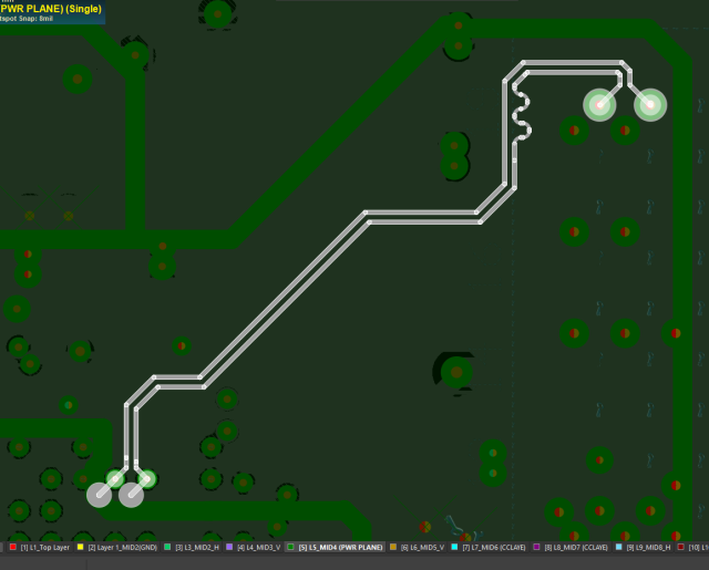
Stackup Design: The Backbone of Controlled Impedance PCB Performance
A reliable Controlled Impedance PCB starts with a stackup engineered around signal integrity rather than cost alone. Controlled dielectric spacing, symmetric layer construction, and uninterrupted reference planes are mandatory. Inconsistent prepreg thickness or reference plane transitions will directly translate into impedance variation and return-path discontinuities.
Professional Controlled Impedance PCB stackups are designed with manufacturing tolerances in mind, ensuring impedance targets remain stable during volume production.
Material Selection and Dielectric Control
Dielectric stability is a decisive factor in Controlled Impedance PCB performance. High-speed and RF applications demand laminates with tight Dk tolerance, low dissipation factor (Df), and minimal frequency dispersion. Variations in resin content, glass weave effects, and thermal expansion can all degrade impedance consistency.
For advanced Controlled Impedance PCB designs, material selection is as important as routing accuracy.
Differential Impedance Control and Signal Symmetry
Differential Controlled Impedance PCB routing requires more than matched trace widths. Differential impedance stability depends on coupling consistency, length matching, symmetric reference planes, and identical via transitions. Any imbalance converts differential signals into common-mode noise, increasing EMI and reducing signal fidelity.
Via Design and Impedance Discontinuity Management
Vias introduce unavoidable impedance discontinuities in Controlled Impedance PCB layouts. Backdrilling, optimized antipads, short via stubs, and nearby ground stitching vias are essential techniques to preserve impedance continuity. Poor via design is one of the most common causes of signal integrity failure in otherwise well-designed Controlled Impedance PCBs.
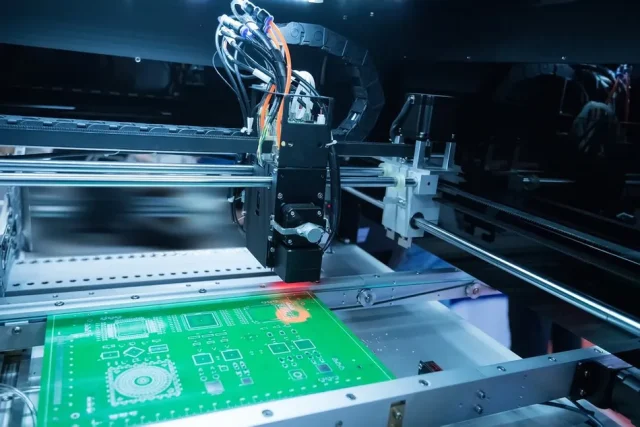
Manufacturing Tolerances and Impedance Accuracy
True Controlled Impedance PCB fabrication accounts for real-world process variation, including copper plating thickness, etch factor, and dielectric tolerance. Engineering-grade designs define impedance tolerance budgets rather than ideal values, typically targeting ±10%, ±7%, or ±5% depending on application sensitivity.
Designs that ignore fabrication realities often fail impedance testing despite correct simulation results.
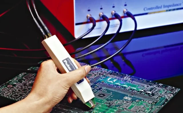
Impedance Testing and Validation
Controlled Impedance PCB verification relies on Time Domain Reflectometry (TDR) measurements using impedance coupons that replicate the actual PCB stackup and trace geometry. Accurate testing confirms that theoretical impedance targets are achieved consistently across production panels.
Applications of Controlled Impedance PCB Technology
Controlled Impedance PCB solutions are essential in:
-
High-speed digital interfaces (PCIe, Ethernet, USB, HDMI)
-
RF transceiver and antenna feed networks
-
5G, mmWave, and satellite communication systems
-
Industrial automation and high-speed control electronics
In these systems, impedance accuracy directly affects performance, reliability, and regulatory compliance.
KKPCB Controlled Impedance PCB Capabilities
KKPCB delivers Controlled Impedance PCB solutions through stackup-driven design, advanced material selection, impedance simulation, and production-level impedance validation. By integrating engineering analysis with manufacturing expertise, KKPCB ensures stable impedance performance from prototype to mass production.
