
Engineering Context
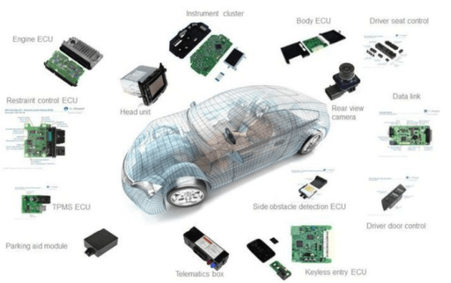
The rapid expansion of autonomous driving systems and new energy vehicles (NEVs) is fundamentally reshaping automotive electronics architecture. Modern vehicles are no longer purely mechanical systems but highly integrated electronic platforms relying on advanced PCB technologies for sensing, decision-making, and power control.
In China, the acceleration of electric mobility and intelligent driving systems has driven significant innovation in automotive-grade PCB design, particularly in areas such as ADAS (Advanced Driver Assistance Systems), radar sensing, battery management systems (BMS), and domain controller architectures.
These systems require PCBs that can support high-frequency radar signals, high-speed digital processing, and high-current power distribution within a single compact multilayer structure. Signal integrity, EMI suppression, thermal stability, and mechanical reliability become critical engineering constraints in automotive environments characterized by vibration, humidity, and extreme temperature variation.
KKCPB develops automotive PCB solutions optimized for sensor fusion platforms, autonomous driving compute modules, and NEV power control systems, ensuring stable electrical performance under complex operating conditions.
Core Engineering Challenges
| Engineering Challenge | Root Cause | System Impact |
|---|---|---|
| Radar signal distortion | Dielectric instability and impedance mismatch | Reduced object detection accuracy |
| EMI interference in sensor fusion | High-density mixed-signal routing | False detection and data corruption |
| Thermal stress in EV systems | High power density and poor heat dissipation | Reduced reliability and lifespan |
| Signal delay in high-speed buses | Long interconnect paths and stackup imbalance | Timing errors in ADAS decisions |
| Mechanical vibration fatigue | Road conditions and engine vibration | Via cracking and solder joint failure |
These challenges are amplified in autonomous driving platforms where multiple sensing modalities must operate in real-time with extremely low latency.
Material Science & Automotive PCB Requirements
Automotive PCBs require materials that maintain stable electrical performance under harsh environmental and electrical stress conditions.
Key Automotive PCB Material Parameters
| Parameter | Engineering Requirement | Benefit |
|---|---|---|
| Low Loss Dielectric (Df) | Stable high-frequency performance | Reliable radar operation |
| Controlled Dk Stability | Minimal variation under heat | Accurate impedance control |
| High Tg Materials | >170°C class or higher | Lead-free solder reliability |
| Low CTE | Thermal expansion control | Reduced warpage |
| Moisture Resistance | Long-term stability | Prevents dielectric drift |
Advanced materials such as RO4003C, RO4350B, Megtron 6/7, ceramic composites, and high-Tg FR-4 systems are widely used in automotive electronic PCB architectures.
KKCPB Case Study — Autonomous Driving Sensor Fusion & Automotive Radar PCB Platform
Client & Application Context
A leading automotive electronics Tier-1 supplier required a high-reliability PCB platform for an autonomous driving domain controller integrating:
- 77–81 GHz automotive radar modules
- Camera and LiDAR sensor fusion interfaces
- High-speed CAN FD and Ethernet communication
- AI-based edge computing processor
- Battery management system (BMS) interface
The PCB needed to support both mmWave radar signal integrity and high-speed digital processing within a compact multilayer architecture.
Engineering Problem
Initial PCB prototypes exhibited several critical issues:
- Radar phase deviation up to 1.8° under thermal cycling
- EMI coupling between radar and camera processing channels
- Impedance mismatch in high-speed Ethernet lanes (±6%)
- Thermal hotspots near power distribution zones
- Mechanical stress-induced via fatigue under vibration testing
These issues resulted in unstable sensor fusion output and inconsistent object detection accuracy.
KKCPB Engineering Solution
KKCPB implemented a multi-domain automotive PCB optimization strategy:
- Adoption of low-loss RF materials for radar signal layers
- Hybrid stackup combining RF, high-speed digital, and power domains
- Controlled impedance routing with ±2% tolerance
- Dedicated EMI isolation architecture between sensor domains
- Optimized copper balancing for thermal uniformity
- Reinforced via structures for vibration resistance
- Thermal via arrays for high-power zones (BMS and compute units)
Measured Results
| Parameter | Baseline Design | KKCPB Optimized PCB |
|---|---|---|
| Radar Phase Stability | ±1.8° | ±0.45° |
| Impedance Variation | ±6% | ±1.8% |
| EMI Coupling Level | High | Reduced by 40% |
| Thermal Hotspot Temperature | High | Reduced by 7°C |
| Via Fatigue Failure Rate | Present | Eliminated |
| System Reliability Index | Medium | High |
Outcome
The optimized automotive PCB platform significantly improved autonomous driving system stability. Radar detection accuracy was enhanced through improved phase consistency, while sensor fusion reliability was strengthened through EMI suppression and impedance control.
From a system integration perspective, the improved thermal management and mechanical reliability extended operational lifespan and reduced field failure risk in real-world driving conditions.
Stackup Design & RF Implementation
Automotive Autonomous Driving PCB Stackup
| Layer | Function | Material |
|---|---|---|
| L1 | Automotive Radar RF Layer | Low-loss RF laminate |
| L2 | Ground Shield | Copper |
| L3 | High-speed Sensor Data | Megtron / High-Tg material |
| L4 | Power Distribution | High-current copper plane |
| L5 | Sensor Fusion Interface | High-speed material |
| L6 | Ground Reference | Copper |
| L7 | Control System Layer | High-Tg FR-4 |
| L8 | Power/BMS Layer | Reinforced high-Tg material |
Simulation & Validation
HFSS Electromagnetic Simulation
- Radar antenna feed optimization
- EMI coupling suppression analysis
ADS RF Simulation
- S-parameter tuning for mmWave radar paths
- Phase stability optimization
TDR Analysis
- Impedance discontinuity correction
- High-speed bus validation
Thermal FEM Simulation
- EV power distribution heat mapping
- Sensor module thermal drift modeling
Environmental & Reliability Validation
| Test | Condition | Result |
|---|---|---|
| Thermal Cycling | -40°C to +125°C | Stable radar phase |
| Vibration Test | 5–500 Hz, 10G | No via or solder failure |
| Humidity Test | 85°C / 85% RH | No dielectric drift |
| Solder Reflow | 260°C ×3 cycles | No warpage |
| Mechanical Shock | Automotive standard | Structural integrity maintained |
| EMI Compliance | System-level testing | Passed with margin |
Engineering Summary & Contact
China’s rapid advancement in autonomous driving and new energy vehicle technologies is driving significant innovation in automotive PCB engineering. High-frequency radar integration, sensor fusion architectures, and EV power systems require PCBs with exceptional electrical stability, thermal reliability, and EMI control.
KKCPB provides advanced automotive PCB engineering solutions for autonomous driving and NEV platforms, integrating low-loss RF materials, controlled impedance stackups, and system-level simulation validation to ensure high-performance and reliable operation.
For automotive radar PCB design, sensor fusion platform development, and NEV high-reliability PCB manufacturing, contact KKCPB Engineering Team for customized engineering and production support.
