What Is a Blind Via PCB?
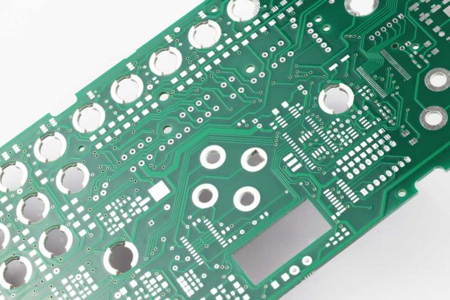
A Blind Via PCB is a multilayer PCB that contains vias connecting an outer layer to one or more inner layers without going through the entire board. Unlike through-hole vias, blind vias enable high-density routing and space-saving designs, which are critical for HDI PCBs, high-frequency applications, and compact electronics.
Blind vias are commonly used in 5G routers, ADAS PCBs, RF Test PCBs, and high-speed computing boards.
Key Advantages of Blind Via PCB
Using a Blind Via PCB offers several advantages:
-
Higher routing density for complex multilayer designs
-
Reduced board size by saving space for traces and components
-
Improved signal integrity by minimizing stub lengths
-
Better high-speed and high-frequency performance
-
Enhanced reliability in HDI and compact PCB designs
These benefits make blind vias essential for modern high-speed and high-frequency electronics.
Design Considerations for Blind Via PCB
Designing a blind via PCB requires careful attention:
-
Via diameter and aspect ratio to ensure proper plating
-
Via location and spacing to optimize routing density
-
Stack-up design to maintain signal integrity and impedance
-
Thermal and mechanical stress management
-
Controlled depth drilling to prevent inner layer damage
Proper design ensures high reliability and stable performance in multilayer PCBs.
Manufacturing Challenges for Blind Via PCB
Producing blind via PCBs involves advanced processes:
-
Laser or mechanical drilling for precise blind via formation
-
High-quality plating to ensure conductivity
-
Layer registration control for multilayer HDI boards
-
Via filling (optional) for planar surfaces or thermal management
-
Inspection and electrical testing to verify reliability
Only experienced HDI PCB manufacturers can consistently produce high-quality blind via PCBs.
Applications of Blind Via PCB
Blind via PCBs are widely used in:
-
5G router and communication PCBs
-
ADAS and automotive sensor modules
-
High-frequency sensor and RF test PCBs
-
Smartphones, wearables, and compact consumer electronics
-
High-speed computing and networking boards
They are ideal wherever high routing density and signal integrity are required.
Conclusion
A Blind Via PCB enables high-density, high-speed, and high-frequency PCB designs by allowing precise layer connections without full board penetration. Its adoption is critical for HDI, 5G, automotive, and advanced electronics applications.
Partnering with a professional Blind Via PCB manufacturer ensures precise drilling, consistent plating, stable impedance, and reliable performance from prototype to volume production.
