What Is an ATE Test PCB?
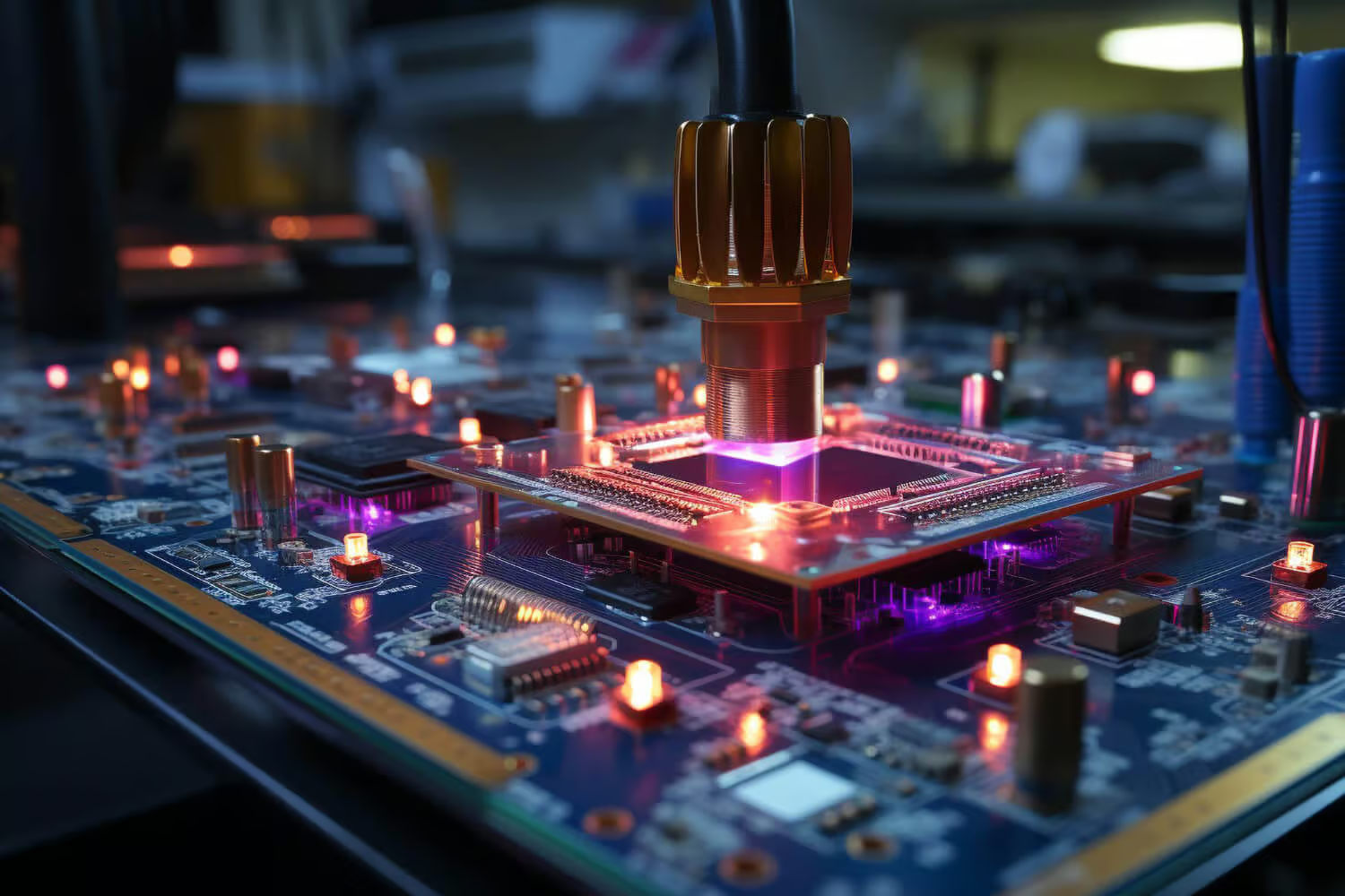
An ATE Test PCB is a specialized printed circuit board used in Automated Test Equipment (ATE) systems to perform functional, parametric, and reliability testing of semiconductor devices.
ATE test boards act as the electrical interface between the testing machine and the device under test (DUT). They ensure accurate signal transmission, stable power delivery, and repeatable measurement results during high-volume production.
The Role of ATE Test PCB in Semiconductor Manufacturing
In semiconductor production, every IC must be validated before shipment. ATE systems perform:
-
Functional testing
-
Performance characterization
-
Parametric measurements
-
High-speed interface verification
-
Burn-in screening
The test PCB must maintain signal accuracy and mechanical stability across thousands of test cycles.
Key Design Requirements
1. High Signal Integrity
ATE test boards often support:
-
High-speed SERDES interfaces
-
RF signal paths
-
Differential pairs
-
High-frequency clocks
Controlled impedance routing and low-loss materials are essential to prevent signal distortion.
2. High Reliability Under Repeated Use
ATE boards are subject to:
-
Frequent DUT insertion and removal
-
Thermal cycling
-
Mechanical stress
-
Long production shifts
Durable surface finishes and reinforced pad structures improve lifetime.
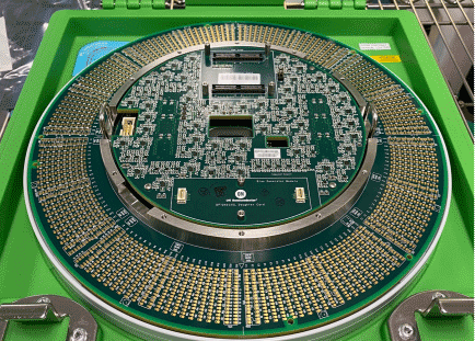
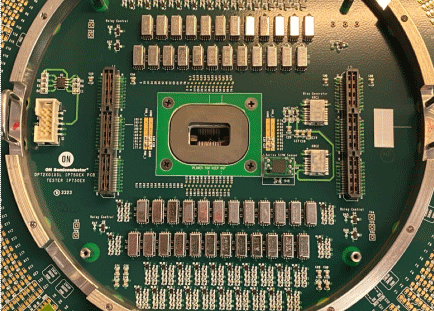
3. Precise Socket and Probe Interface
ATE boards must integrate with:
-
Test sockets
-
Probe pins
-
Spring contacts
-
High-speed connectors
Accurate alignment and robust pad design are critical to ensure stable contact resistance.
4. Power Integrity
Modern ICs require multiple voltage rails with tight tolerance. ATE test PCBs incorporate:
-
Dedicated power planes
-
Decoupling networks
-
Low impedance current paths
-
Thermal vias for heat dissipation
Stable power delivery ensures accurate measurement results.
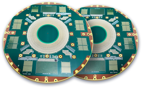
Material and Stack-Up Considerations
Depending on the application, ATE test PCBs may use:
-
Standard FR4 for low-speed logic testing
-
Low-loss materials for high-frequency testing
-
Hybrid stack-ups for cost-performance balance
Multilayer and HDI structures are common in advanced ATE platforms.
Applications of ATE Test PCB
ATE test PCBs are widely used in:
-
Microcontroller testing
-
RF transceiver validation
-
5G chip production
-
Memory device testing
-
Automotive IC qualification
-
IoT semiconductor testing
-
AI and data center chip validation
They are essential for ensuring yield and product reliability in mass production.
ATE Test PCB vs Load Board
| Feature | ATE Test PCB | Load Board |
|---|---|---|
| Purpose | Functional & parametric test | Interface & signal distribution |
| Integration | Direct ATE system interface | Often used within test setup |
| Frequency Range | Low to mmWave | Depends on application |
| Mechanical Durability | Very High | High |
| Production Usage | Mass production | Engineering & production |
ATE test PCBs are optimized for repeated automated testing and high-volume manufacturing environments.
Conclusion
ATE Test PCB technology is a critical component in semiconductor testing and mass production. With strong emphasis on signal integrity, mechanical durability, and power stability, it ensures accurate, repeatable, and reliable device validation.
As semiconductor performance continues to advance into higher frequencies and greater integration levels, precision ATE test board design becomes increasingly important for maintaining production yield and product quality.
