What Is an ATE Test PCB?
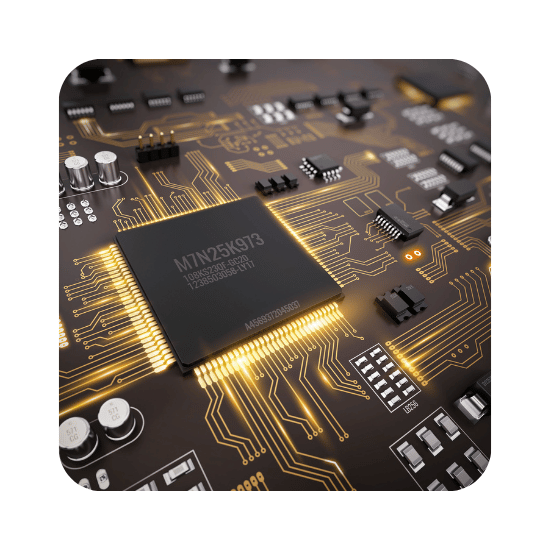
An ATE Test PCB is a specialized printed circuit board designed for use in Automated Test Equipment (ATE) systems. It acts as the electrical interface between semiconductor devices and the test platform, enabling accurate signal transmission, power delivery, and measurement during IC testing.
ATE Test PCB is commonly used in:
-
Wafer testing
-
Final package testing
-
Burn-in testing
-
Functional IC testing
-
High speed digital validation
In semiconductor manufacturing, ATE Test PCB plays a critical role in ensuring device reliability and performance before shipment.
Key Functions of ATE Test PCB
1. Signal Routing and Integrity
ATE Test PCB must support:
-
High speed digital signals
-
RF signal transmission
-
Differential pair routing
-
Controlled impedance traces
Maintaining signal integrity is essential to prevent data errors during high frequency and high bandwidth testing.
2. Power Distribution
ATE Test PCB delivers stable and low-noise power to the device under test (DUT). It must handle:
-
Multiple voltage domains
-
High current paths
-
Low impedance power planes
Stable power ensures accurate electrical characterization.
3. High Pin Count Interconnection
Modern semiconductor devices often feature:
-
High pin count BGA packages
-
Fine pitch interfaces
-
Dense I/O requirements
ATE Test PCB supports complex routing structures such as buried vias, blind vias, and HDI layouts to manage high interconnection density.
4. Mechanical Stability
ATE Test PCB must withstand:
-
Repeated insertion cycles
-
Thermal stress
-
Long test durations
High reliability materials and precise fabrication are critical for consistent test results.
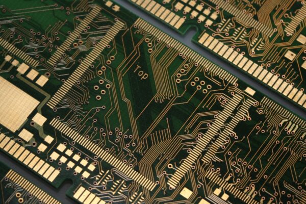
Technical Capabilities of ATE Test PCB
ATE Test PCB manufacturing may include:
-
8–40+ layer multilayer PCB
-
High TG or low loss materials
-
Controlled impedance routing
-
Back drilling to remove via stubs
-
Fine line and fine pitch processing
-
Heavy copper for high current testing
-
Sequential lamination for HDI structures
Strict electrical testing ensures signal continuity and impedance compliance.
Applications of ATE Test PCB
ATE Test PCB is widely used in:
-
Logic IC testing
-
Memory device testing
-
RF IC testing
-
Automotive chip validation
-
Power semiconductor testing
-
5G communication chip testing
As semiconductor technology advances, ATE Test PCB requirements continue to increase in complexity and precision.
ATE Test PCB vs Standard PCB
| Feature | ATE Test PCB | Standard PCB |
|---|---|---|
| Application | Semiconductor Testing | General Electronics |
| Signal Speed | Very High | Moderate |
| Pin Density | Extremely High | Standard |
| Impedance Control | Strict | Optional |
| Reliability Requirement | Critical | Normal |
ATE Test PCB is engineered specifically for high accuracy and high reliability testing environments.
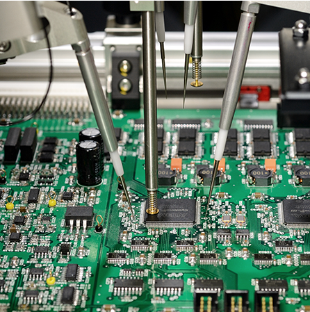
Manufacturing Challenges
Producing ATE Test PCB requires:
-
Tight impedance tolerance control
-
High layer alignment accuracy
-
Precise via plating quality
-
Stable dielectric materials
-
Comprehensive electrical inspection
An experienced ATE Test PCB manufacturer ensures high yield and consistent performance for semiconductor test systems.
Conclusion
ATE Test PCB is a core component in semiconductor testing infrastructure. It enables precise signal transmission, stable power distribution, and reliable device evaluation in Automated Test Equipment systems.
With increasing IC complexity and higher data speeds, ATE Test PCB technology must continuously evolve to support advanced testing requirements.
Selecting a professional ATE Test PCB supplier ensures accuracy, durability, and long-term performance in demanding semiconductor environments.
