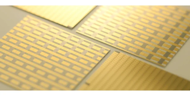
An Aluminum Nitride (AlN) PCB is a printed circuit board built using aluminum nitride substrates, which provide high thermal conductivity (up to 170–200 W/m·K) and excellent electrical insulation. These properties make AlN PCBs ideal for high-power devices, RF circuits, and applications requiring efficient heat dissipation in compact layouts.
AlN PCBs are commonly used in:
-
Power electronics and high-current modules
-
RF and microwave circuits
-
LED lighting and optoelectronic devices
-
Aerospace and defense electronics
The primary advantage of AlN PCBs is their ability to rapidly conduct heat away from critical components, preventing thermal degradation and improving long-term reliability.
Thermal & Electrical Challenges
Designing AlN PCBs requires addressing several technical challenges:
-
Thermal Management: High-power circuits generate localized hotspots; effective heat dissipation is critical to avoid component failure.
-
Coefficient of Thermal Expansion (CTE) Mismatch: Differences between AlN substrate and copper or component materials can induce mechanical stress during thermal cycling.
-
Signal Integrity for High-Frequency Applications: RF and microwave signals require careful trace design and impedance control on ceramic substrates.
-
Manufacturability: AlN is brittle and requires specialized processing to avoid cracking or chipping during drilling and lamination.
Design & Material Solutions
Engineers employ several strategies to overcome these challenges:
-
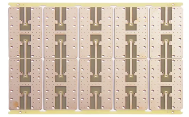
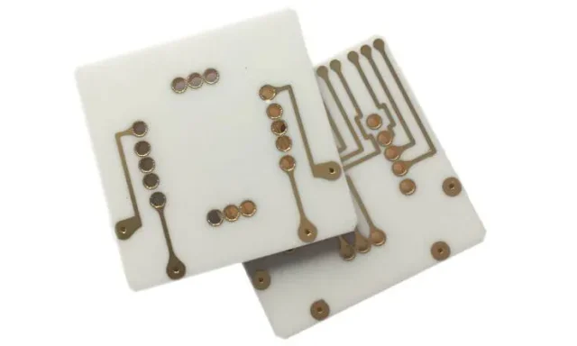
Copper Clad Aluminum Nitride: Copper layers are bonded to AlN substrates for both electrical connectivity and enhanced heat spreading.
-
Thermal Via Integration: Vias transfer heat from top-side components to the substrate or heat sink efficiently.
-
Controlled Trace Layouts: Microstrip or coplanar waveguide designs maintain signal integrity in high-frequency applications.
-
CTE Compensation Techniques: Proper selection of solder materials and component pads minimizes mechanical stress.
-
Layer Stack-Up Optimization: Single- or double-sided AlN designs are tailored to balance electrical, thermal, and mechanical performance.
Fabrication Considerations
AlN PCB manufacturing requires precision and specialized techniques:
-
Substrate Preparation: AlN ceramics are sintered with high density to achieve consistent thermal conductivity and mechanical strength.
-
Copper Lamination & Etching: High-quality copper foils are bonded and patterned with care to prevent substrate cracking.
-
Drilling & Plating: Laser or ultrasonic drilling is used for microvias, followed by metallization for electrical connectivity.
-
Surface Finishes: ENIG or silver finishes are applied to protect fine traces and improve solderability.
-
Quality Assurance:
-
Thermal performance testing ensures heat dissipation meets design requirements
-
Electrical testing verifies continuity and impedance in high-frequency circuits
-
Mechanical inspections detect cracks, delamination, or substrate defects
-
KKPCB implements these processes to produce AlN PCBs with reliable thermal and electrical performance under high-power or high-frequency conditions.
Applications
AlN PCBs are essential for applications demanding high thermal efficiency and signal reliability:
-
Power Electronics: High-current DC–DC converters, power amplifiers, and motor controllers
-
RF & Microwave Circuits: Antennas, filters, and transceivers operating at GHz frequencies
-
LED & Laser Modules: Efficient heat spreading for high-power optoelectronic devices
-
Aerospace & Defense Systems: Avionics and radar modules requiring high reliability under thermal stress
-
Test & Measurement Equipment: High-power diagnostic and RF instrumentation
By leveraging high-thermal-conductivity substrates, controlled trace design, thermal vias, and precise fabrication, KKPCB delivers AlN PCBs capable of performing reliably in demanding electronic systems where heat and signal integrity are critical.
