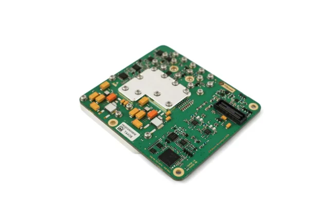
Energy Storage Systems (ESS)—from large-scale Battery Energy Storage Systems (BESS) to EV battery packs, industrial UPS units, and hybrid inverters—operate under sustained electrical and thermal stress. High charging currents, repeated load cycles, and fast switching from power semiconductors all demand a PCB platform that can withstand extreme conditions without degradation.
This is exactly where Heavy Copper PCB architectures deliver long-term reliability. By integrating 3oz–20oz copper weights into multilayer structures, these power boards provide the mechanical strength, thermal efficiency, and current-carrying capacity that modern ESS hardware requires.
Why Heavy Copper PCBs Are Critical for ESS Power Platforms
1. High Current Carrying Capacity for Power Switching Stages
ESS systems rely on MOSFETs, IGBTs, GaN, or SiC devices operating at high current density. Heavy Copper PCBs enable:
• Lower resistive losses along power rails
• Wider, reinforced traces for 50–400 A loads
• Stable operation during fast charge/discharge events
With 4oz–10oz conductors, trace temperature rise is dramatically reduced, improving long-term operational stability.
2. Superior Thermal Management for Heat-Intensive Modules
Thermal runaway is a major reliability threat in ESS platforms. Heavy Copper PCB stackups improve heat dissipation through:
• Thick copper planes functioning as integrated heat spreaders
• Efficient thermal pathways from power devices to heatsinks
• Reduced hotspot formation during peak current surges
In SiC-based ESS converters, heavy copper layers help maintain junction temperatures within safe limits—even during extreme load transitions.
3. Long-Term Mechanical Integrity Under Continuous Stress
ESS boards frequently experience mechanical strain caused by large currents, high voltage isolation requirements, and thermal cycling. Heavy Copper PCBs provide:
• Stronger adhesion between copper and dielectric
• Highly robust plated-through holes for repetitive cycling
• Better resistance to vibration and thermal fatigue
This mechanical durability ensures multi-year operational lifespan, even in harsh industrial or outdoor environments.
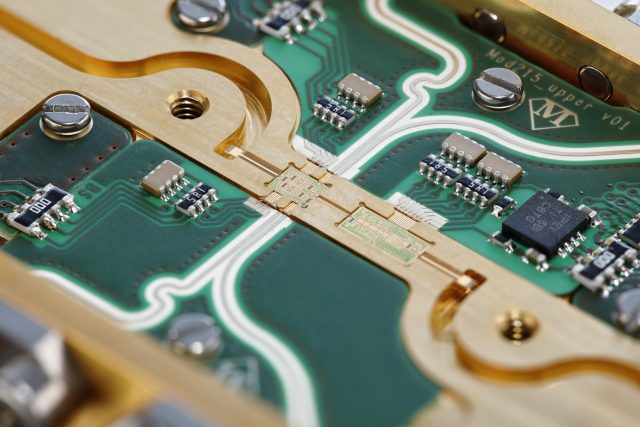
4. Reliable Power Distribution in Multi-Layer ESS Architectures
Modern battery management and inverter systems require multilayer stackups with isolated power, sensing, and control domains. Heavy Copper PCB designs allow:
• Embedded copper coins for ultra-high current paths
• Hybrid stackups combining 2oz signal layers with 6oz–10oz power layers
• Stable impedance control for current sensing channels
This balance of power density and signal integrity is essential for accurate, safe battery system operation.
KKPCB’s Engineering Capabilities for Heavy Copper PCBs
KKPCB specializes in advanced Heavy Copper PCB manufacturing designed specifically for ESS environments, including:
• 3oz–20oz copper plating with uniform distribution
• Deep-plated vias for high-current interconnections
• Differential copper thickness between layers
• High-Tg, FR-4, and hybrid resin systems optimized for thermal stress
• IPC-6012 Class 3 and Class 3A reliability standards
Every ESS Heavy Copper PCB is engineered for maximum mechanical endurance and thermal reliability.
Conclusion
As energy storage technology scales toward higher density, faster charging, and longer service lifecycles, the demands placed on PCB architectures only increase. Heavy Copper PCB stackups offer the electrical robustness, heat dissipation, and mechanical strength required for long-term ESS reliability.
By leveraging KKPCB’s engineered heavy-copper solutions, manufacturers can build safer, more efficient, and more durable ESS platforms capable of supporting the next generation of power electronics.
