RF Test PCB: Engineering Precision for High-Frequency Testing Applications
Introduction
As wireless communication, semiconductor devices, and high-frequency electronics continue to advance, the demand for precise and reliable test platforms has increased dramatically. Among these platforms, the RF Test PCB plays a central role. It enables engineers to validate RF performance, measure high-frequency characteristics, and ensure that devices meet system-level specifications before deployment.
An RF Test PCB is not simply a standard printed circuit board—it is a precision-engineered test interface built to preserve signal integrity across frequencies that can exceed several gigahertz.
What Is an RF Test PCB?
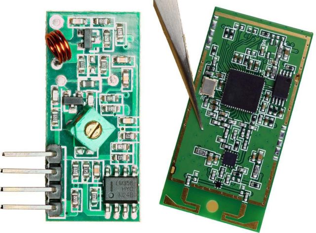
An RF Test PCB is a specialized high-frequency circuit board designed to connect DUTs (Devices Under Test) to RF measurement instruments such as spectrum analyzers, network analyzers, ATE systems, and high-frequency probe stations.
Its goals are:
-
Maintain accurate RF signal transmission
-
Ensure controlled impedance (usually 50 Ω / 100 Ω)
-
Minimize loss, reflection, and phase distortion
-
Provide stable mechanical structure for repeated testing
-
Support precise calibration and repeatability
RF Test PCBs are essential for validating wireless modules, RF chips, power amplifiers, LNA circuits, antennas, and semiconductor wafers.
Key Engineering Requirements of RF Test PCBs
1. Impedance Control
At RF frequencies, trace impedance directly affects measurement accuracy.
Typical targets include:
-
50 Ω single-ended
-
100 Ω differential
To maintain these values, RF Test PCBs require:
-
Tight dielectric thickness control
-
Precise trace width and spacing
-
Continuous ground reference planes
-
Smooth copper profiles to reduce RF losses
Even a small deviation may cause mismatches and S-parameter errors.
2. Signal Integrity Optimization
RF Test PCBs must address:
-
Reflection (S11)
-
Insertion loss (S21)
-
Crosstalk
-
Return path discontinuities
Techniques include:
-
GSG (Ground-Signal-Ground) routing
-
Minimized via count on RF paths
-
Back-drilling to remove via stubs
-
Tapered transitions for connectors and launches
3. Material Selection
Material properties dominate RF behavior.
Common RF test materials include:
-
Rogers RO4350B / RO4003C
-
RO3003 / RO3010
Critical material characteristics:
| Parameter | Requirement |
|---|---|
| Dielectric Constant (Dk) | Stable and predictable |
| Loss Tangent (Df) | Ultra-low loss for GHz use |
| CTE Stability | Prevents warpage and misalignment |
| Moisture Absorption | Extremely low for consistent RF behavior |
These ensure repeatable measurements in a controlled RF test environment.
4. Connector & Launch Design
RF Test PCBs rely on high-performance connectors such as:
-
SMA
-
2.92 mm (K-type)
-
2.4 mm / 1.85 mm
-
Custom ATE test interfaces
Launch geometry must be optimized to:
-
Reduce transition loss
-
Maintain impedance
-
Ensure phase stability
5. High-Frequency Manufacturing Precision
Manufacturing tolerances dramatically affect RF Test PCB performance. KKPCB implements:
-
Laser-drilled microvias
-
Back-drilling
-
Tight copper thickness control
-
Cleanroom lamination
-
Automated optical registration
This guarantees accuracy across repeated test cycles.
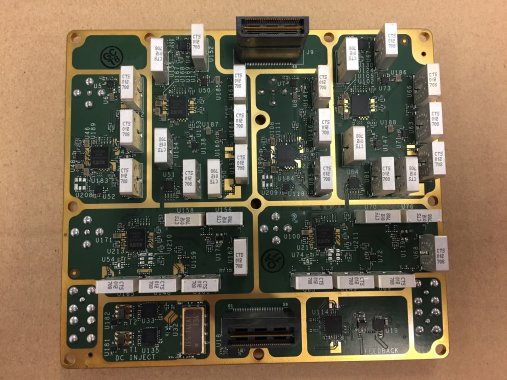
Applications of RF Test PCBs
1. Semiconductor RF Testing
-
RF front-end ICs
-
LNAs, PAs, mixers
2. Wireless Communication
-
5G FR1 / FR2 test modules
-
Antenna testing
3. Automotive Radar
-
24 GHz / 77 GHz module validation
-
Radar SoC characterization
4. Aerospace & Defense
-
Sat-com transceivers
-
High-frequency power modules
Why KKPCB for RF Test PCBs?
KKPCB integrates engineering expertise with high-frequency fabrication capabilities:
-
Controlled impedance manufacturing
-
HDI + low-loss laminate stackups
-
High-precision connector launches
-
Full test and inspection for consistency
We support prototypes and mass production for global RF customers.
Conclusion
An RF Test PCB is a high-precision tool designed to preserve signal integrity and measurement accuracy at high frequencies. As wireless, radar, and semiconductor technologies grow more advanced, the need for reliable RF test platforms becomes critical. With advanced materials, precise fabrication, and deep RF engineering experience, KKPCB delivers RF Test PCBs that ensure accurate, repeatable, and industry-leading performance.
