Signal Integrity — The Invisible Backbone of mmWave Performance
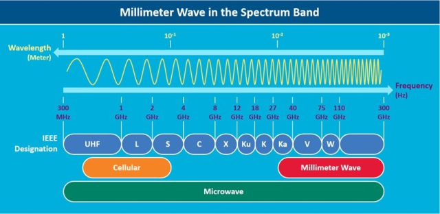
As 5G networks and radar systems transition into 24–77 GHz mmWave frequencies, signal integrity (SI) has become one of the most critical yet challenging aspects of RF PCB engineering.
At these frequencies, every micron of copper geometry, dielectric uniformity, and via structure directly influences insertion loss, phase shift, and system-level beamforming accuracy.
Even a 5 µm etching deviation or 0.02 change in dielectric constant (Dk) can shift antenna phase alignment by 1–1.5°, causing degraded EVM (Error Vector Magnitude) and reduced link efficiency.
That’s why engineers in RF power modules, phased-array systems, and radar transceivers rely on Rogers RO4003C PCB — a proven material combining:
-
Stable Dk = 3.55 ± 0.05
-
Low loss tangent Df = 0.0027 @ 10 GHz
-
Consistent dielectric uniformity
-
Ease of manufacturing vs. PTFE-based laminates
Yet, even the best material cannot deliver reliable SI without precise process control and structure-level optimization.
This is where KKPCB’s high-frequency manufacturing discipline transforms design intent into production-grade RF consistency.
Why RO4003C Excels in mmWave and RF Power Applications
| Property | Typical Value | Design Benefit |
|---|---|---|
| Dielectric Constant (Dk @ 10 GHz) | 3.55 ± 0.05 | Predictable impedance in multi-layer RF stackups |
| Dissipation Factor (Df @ 10 GHz) | 0.0027 | Low insertion loss at 24–77 GHz |
| Thermal Coefficient of Dk | +40 ppm/°C | Stable performance under temperature cycling |
| Tg (Glass Transition Temperature) | >280°C | Excellent mechanical and chemical durability |
These properties make RO4003C a favorite for 5G front-end modules, automotive radar, and satellite phased-array PCBs, where tight impedance tolerance and repeatable RF performance are essential.
Key Signal Integrity Challenges in RO4003C PCB Designs
| Challenge | Root Cause | Engineering Impact |
|---|---|---|
| Impedance Variability | Etching deviation, copper roughness | Phase mismatch, reflection loss |
| Dielectric Inconsistency | Resin flow, hybrid lamination drift | Gain variation, phase delay |
| Via Transition Loss | Discontinuity at microstrip–via junction | Return loss increase |
| Surface Roughness | Copper foil texture & oxide treatment | Additional conductor loss |
| Thermal-Induced Drift | Temperature-dependent Dk shift | Frequency drift under power load |
KKPCB mitigates these through process-driven SI optimization and real-time verification during production.
KKPCB’s Process Framework for Signal Integrity Optimization
1. Controlled Impedance Engineering
At mmWave frequencies, impedance control within ±5% is mandatory to maintain phase alignment across feed networks.
-
Stackup simulation with EM solver (Keysight ADS + HFSS integration)
-
Controlled etching accuracy within ±5 µm
-
Smooth copper foils (Ra < 1.5 µm) to minimize conductor loss
-
In-line impedance verification via 110 GHz VNA calibration
Example:
In a 28 GHz power amplifier test board, optimizing microstrip trace geometry and foil texture reduced return loss by 1.4 dB and improved gain flatness by 8.2% across the band.
2. Hybrid Stackup Design for RF + Power Integration
High-power mmWave systems often combine RO4003C for RF signal layers and FR-4 or Cu cores for power or control planes.
But mismatched CTE (Coefficient of Thermal Expansion) or resin compatibility can induce impedance drift or delamination.
-
Balanced stackup with symmetric RO4003C layers
-
Stepwise lamination at 180°C / 60 min / 200 psi
-
Real-time dielectric thickness validation (±8 µm tolerance)
-
Controlled resin flow analysis using 3D thermal models
Outcome:
Impedance stability improved from ±9% → ±3.5%, verified post-lamination by time-domain reflectometry (TDR).
3. Via Design and Transition Optimization
Via transitions introduce parasitic inductance and capacitance that distort signal phase.
At 39 GHz, an uncompensated via stub can add up to 0.5 dB of insertion loss.
-
Use of back-drilled vias to eliminate stubs
-
Controlled via pad size and anti-pad clearance tuning
-
Resin-filled and capped vias for smoother transitions
-
VNA-based de-embedding to verify S11/S21 continuity
Result:
Insertion loss reduced by 0.18 dB @ 39 GHz, with consistent via impedance across all test coupons.
4. Copper Roughness & Surface Finish Control
Copper roughness (Ra) directly influences high-frequency conductor loss.
KKPCB employs low-profile rolled copper and oxide-free bonding treatment, achieving:
-
Loss reduction up to 15% @ 28 GHz
-
Improved phase linearity under load
-
Better repeatability across production lots
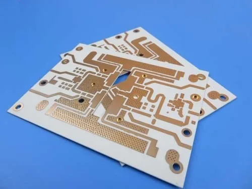
RO4003C PCB
Case Study: 77 GHz Automotive Radar Front-End Module
A Tier-1 automotive radar supplier collaborated with KKPCB to produce a 77 GHz radar transceiver PCB using RO4003C + FR-4 hybrid stackup.
Design Objectives:
-
Maintain impedance variation < ±5%
-
Reduce insertion loss below 0.3 dB/inch
-
Ensure phase consistency across 16-channel array
-
Optimized RF stackup using 0.203 mm RO4003C core
-
Back-drilled vias for feed network uniformity
-
Smooth rolled copper foil and laser-controlled etching
-
RF VNA testing up to 110 GHz on all pilot lots
Results:
| Parameter | Before KKPCB | After KKPCB |
|---|---|---|
| Insertion Loss @ 77 GHz | 0.34 dB/inch | 0.27 dB/inch |
| Impedance Variation | ±8.9% | ±3.8% |
| Beam Alignment Error | 2.1° | 0.6° |
| Yield Improvement | — | +11.5% |
Conclusion:
KKPCB’s precision control enabled stable, repeatable signal integrity across 16-channel radar arrays—ensuring high beam accuracy and lower phase noise in real-world automotive conditions.
Engineering Insights — Best Practices for RO4003C SI Optimization
To achieve consistent signal integrity in mmWave and RF power systems, KKPCB recommends:
-
Maintain impedance within ±5% via stackup and etch control
-
Use smooth copper foils (Ra < 2 µm) for low conductor loss
-
Back-drill or cap vias to eliminate stub reflections
-
Simulate hybrid stackups for CTE and dielectric drift behavior
-
Validate every batch with VNA and TDR inspection
KKPCB’s High-Frequency Manufacturing Capabilities
-
110 GHz VNA impedance verification
-
±3°C thermal lamination uniformity
-
Automated resin flow and void inspection
-
IPC Class 3 / IATF 16949 certification
-
Cross-section & impedance correlation testing
KKPCB bridges RF design and volume manufacturing, ensuring your RO4003C PCBs deliver consistent SI and thermal reliability from prototype to mass production.
Conclusion — Engineering mmWave Stability with RO4003C
RO4003C PCBs offer a rare balance of low loss, stable dielectric performance, and manufacturability—ideal for RF front ends, power amplifiers, and radar systems.
Through KKPCB’s signal integrity–focused process control, engineers achieve low reflection, phase stability, and scalable mmWave reliability across every production batch.
Partner with KKPCB for Your Next RO4003C mmWave Project
KKPCB Engineering Team offers:
-
RF signal integrity modeling & validation
-
Stackup and via optimization for mmWave frequencies
-
Batch-level impedance & loss verification
-
Automotive radar & 5G module qualification support
Contact KKPCB Engineering Support to discuss your RO4003C-based RF or mmWave PCB design.
