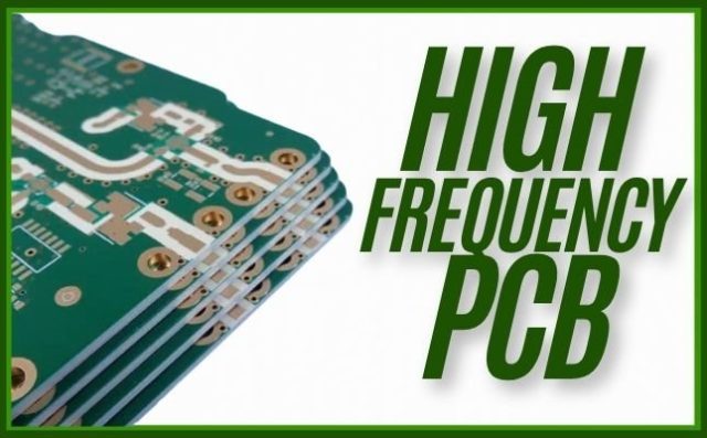
The Fascination of High-Frequency PCBs — Part 1: Engineering Precision and Key Success Factors
In today’s fast-moving digital world, speed is everything. From radar and satellite communication to 5G infrastructure, sensors, and medical electronics — high-frequency (HF) and microwave (MW) circuits define the backbone of wireless innovation.
At KKPCB, we have spent years refining our expertise in the design and manufacture of high-frequency printed circuit boards (RF PCBs), ensuring uncompromising performance where signal precision and material stability matter most. This article provides an inside look at what determines success in HF PCB manufacturing — from signal integrity and material science to the fine art of copper patterning.
1. Understanding High Frequency and PCB Functionality
High frequency generally refers to signal ranges above 10 MHz, where electromagnetic wave behavior introduces new design challenges such as thermal effects and dielectric loss. In PCB design, the typical HF range extends from 10 GHz up to 100 GHz, depending on the application.
In such conditions, the PCB becomes more than a substrate — it becomes a precision transmission element. Each conductor path must be carefully designed to maintain target impedance values, with attention to trace width, dielectric thickness, and distance to reference planes.
At KKPCB, our HF circuit capabilities include components such as couplers, filters, λ/4 structures, antennas, and ring resonators, manufactured with micron-level accuracy.
2. Signal Integrity: The Core of RF Performance
Smooth and precise signal transmission is the heartbeat of every high-frequency design. Even microscopic surface roughness or etching defects can create unwanted signal reflections.
To achieve this, KKPCB controls every conductor path’s contour and surface condition through advanced etching uniformity control and copper surface treatment optimization. According to the skin effect, high-frequency currents flow mainly along the conductor surface — therefore, the smoother the copper, the cleaner the signal.
Our process minimizes copper roughness while maintaining adhesion reliability, achieving a balance between electrical performance and mechanical strength.
3. Material Selection: The Science of Stability
The foundation of every successful HF PCB lies in choosing the right dielectric material. KKPCB engineers evaluate multiple parameters to ensure long-term stability:
-
Dielectric constant (Dk) and dissipation factor (Df)
-
Thermal stability of HF parameters
-
Copper adhesion strength and dimensional stability
-
Moisture resistance and low water absorption
-
Material cost-efficiency
We commonly work with Rogers, Taconic, Isola, and Panasonic substrates and provide hybrid stack-up designs combining PTFE and FR-4 to achieve an optimal balance between performance and cost.
4. Precision in Processing and Fabrication
PTFE and ceramic-based materials used in high-frequency PCBs require highly specialized processing. KKPCB employs dedicated drilling, milling, and lamination parameters — adjusting spindle speed, feed rate, and tool geometry for each substrate type.
Through our CAM simulation and real-time AOI inspection, we ensure dimensional fidelity and defect-free cutting. Edge smoothness and consistency across production panels are verified early in the process to guarantee repeatable impedance performance across all boards.
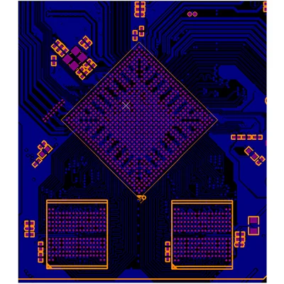
5. Conductor Pattern and Tolerance Control
In RF layouts, minute variations in line width or edge roughness can alter impedance. KKPCB’s fine-line imaging and laser direct imaging (LDI) ensure sharp edge definition with minimal corner rounding.
We verify every HF layer through automated optical inspection (AOI) during the first article production phase — allowing precise parameter adjustments before mass manufacturing.
The result: tight impedance tolerances, stable frequency response, and unmatched reproducibility.
KKPCB — Engineering the Future of High-Frequency PCBs
From concept to production, KKPCB provides complete engineering support for RF, microwave, and high-speed PCB projects. Our team collaborates directly with customers’ R&D engineers, offering guidance on stack-up design, material selection, impedance modeling, and manufacturability optimization.
Whether your project operates at 1 GHz or 77 GHz, KKPCB delivers PCBs that meet the demands of modern communication, radar, and sensing technologies — with precision built into every layer.
