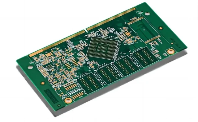
HDI PCB: The Foundation of Modern Electronic Miniaturization
In today’s electronics industry, devices are becoming smaller, faster, and more powerful. To achieve this balance, engineers increasingly rely on HDI PCBs (High-Density Interconnect Printed Circuit Boards)—a technology that allows for higher circuit density, improved signal integrity, and enhanced performance within compact form factors.
At KKPCB, we specialize in advanced HDI PCB manufacturing, providing solutions that meet the demanding requirements of smart devices, automotive electronics, 5G infrastructure, and medical systems.
What Is HDI PCB?
HDI PCBs utilize microvias, laser-drilled blind and buried vias, and ultra-fine trace patterns to achieve significantly higher wiring density than standard multilayer boards. This enables shorter signal paths, lower transmission loss, and higher speed signal transmission—critical factors in modern high-frequency and high-speed digital designs.
An HDI PCB typically includes multiple sequential lamination processes, allowing complex interconnections across layers without increasing board thickness. This structure improves electrical performance, thermal management, and mechanical reliability.
Key Advantages of HDI Technology
1.Compact Design,Greater Functionality:
HDI allows more components and interconnections within a smaller area, enabling the miniaturization of smartphones, tablets, and wearable devices.
2.Improved Signal Integrity:
With shorter interconnects and lower crosstalk, HDI PCBs support high-speed data transfer and low electromagnetic interference (EMI).
3.Enhanced Reliability:
Microvias reduce stress concentration during thermal cycling, improving the board’s fatigue resistance and long-term durability.
4.Design Flexibility:
HDI’s layer-stacking and via-in-pad techniques give engineers more options to route signals efficiently, especially in BGA and fine-pitch IC packaging.
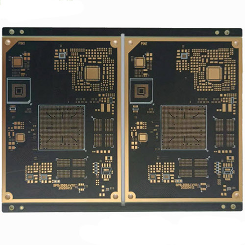
KKPCB’s HDI Manufacturing Capabilities
KKPCB employs state-of-the-art laser drilling, sequential lamination, and precision imaging equipment to produce HDI boards that meet the strictest tolerance standards.
Our capabilities include:
1+N+1 to 3+N+3 HDI stack-up configurations
Via-in-pad and filled microvia plating
Line/space as fine as 50/50 µm (2/2 mil)
Tight impedance control for high-speed signals
Material support: FR-4, Rogers, Megtron 6, and hybrid stack-ups
Through controlled processes and rigorous quality testing, KKPCB ensures every HDI board maintains dimensional stability, dielectric consistency, and repeatable impedance performance—from prototype to mass production.
Applications of HDI PCB
HDI technology has become essential across a wide range of industries:
Consumer Electronics: Smartphones, tablets, and wearables
Telecommunications: 5G modules, RF transceivers, routers
Automotive Electronics: ADAS, radar, infotainment systems
Medical Devices: Imaging systems and implantable sensors
Aerospace & Defense: Compact communication and control systems
In these applications, KKPCB delivers high-density interconnection solutions that balance space efficiency, signal fidelity, and long-term reliability.
Conclusion
As electronic systems continue to evolve toward miniaturization and higher performance, HDI PCBs have become the backbone of next-generation design. KKPCB combines engineering expertise and precision manufacturing to provide customers with reliable, high-density, high-speed PCB solutions tailored to their specific application needs.
