
With the continuous development of smartphones toward higher performance, smaller size, and increased functionality, mobile phone PCB design has become more complex than ever. Modern smartphones integrate high-speed processors, RF communication modules, cameras, sensors, power management circuits, and high-density interconnect structures within extremely limited space.

However, increasing circuit density and operating frequencies also introduce greater challenges related to electromagnetic interference (EMI) and electromagnetic compatibility (EMC).
Poor EMC design may lead to:
- Wireless signal degradation
- Communication interference
- Touchscreen malfunction
- Audio noise
- Reduced battery efficiency
- Failure to pass regulatory certification
Therefore, EMC design must be considered throughout the entire mobile phone PCB development process, from schematic design and stack-up planning to PCB layout and manufacturing.
1. Understanding EMC and EMI in Mobile Phone PCB Design
What Is Electromagnetic Compatibility (EMC)?
Electromagnetic compatibility refers to the ability of an electronic device to operate correctly in its electromagnetic environment without causing unacceptable interference to other devices.
EMC includes two major aspects:
Electromagnetic Interference (EMI)
EMI refers to unwanted electromagnetic energy generated by electronic circuits that may affect nearby components or external devices.
Sources of EMI in mobile phones include:
- High-speed processors
- Clock signals
- Switching power supplies
- RF transmit circuits
- High-speed memory interfaces
Electromagnetic Susceptibility (EMS)
EMS describes a device’s ability to withstand external electromagnetic disturbances without malfunction.
A well-designed mobile phone PCB must both reduce emissions and improve immunity.
2. Main Sources of Electromagnetic Interference in Mobile Phone PCBs
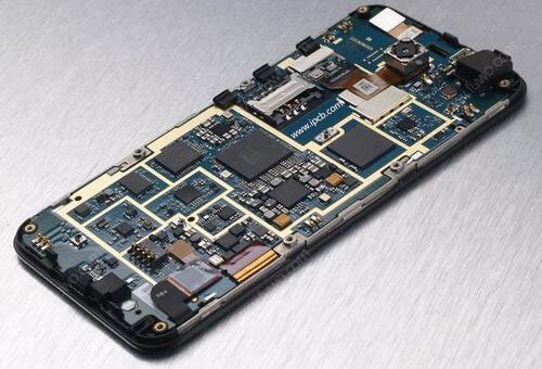
Mobile phone PCBs contain multiple high-frequency circuits operating simultaneously, creating potential EMI risks.
High-Speed Digital Circuits
Modern processors and memory interfaces operate at high frequencies with fast switching edges.
Common EMI sources include:
- CPU clock signals
- DDR memory interfaces
- High-speed serial communication
- Display interfaces
Rapid voltage transitions generate high-frequency harmonic components that can radiate through PCB traces.
RF Communication Circuits
Mobile phones contain multiple wireless systems:
- Cellular communication
- Wi-Fi
- Bluetooth
- GPS
- NFC
RF circuits require strict isolation because unwanted coupling may affect transmission performance and receiver sensitivity.
Power Management Circuits
Switching regulators generate electromagnetic noise due to rapid current changes.
Potential issues include:
- Power ripple
- Conducted noise
- Radiation from current loops
Proper power layout is essential for reducing interference.
3. PCB Stack-Up Design for EMC Performance
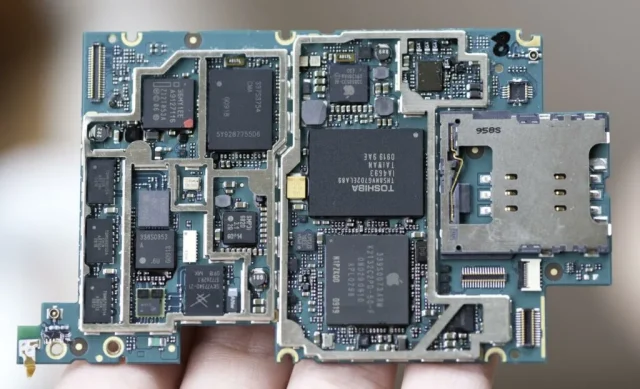
A well-designed PCB stack-up provides a foundation for electromagnetic control.
Use Continuous Reference Planes
Ground planes provide low-impedance return paths for high-frequency currents.
Benefits include:
- Reduced electromagnetic radiation
- Improved signal integrity
- Lower crosstalk
For multilayer mobile phone PCBs, dedicated ground layers are commonly used to improve EMC performance.
Signal Layer Arrangement
High-speed signals should be routed close to reference planes to minimize loop areas.
Recommended practices include:
- Avoid routing sensitive signals across split planes
- Keep high-speed traces adjacent to ground references
- Separate RF and digital signal layers when possible
Layer Isolation
Different functional areas should be properly isolated:
- RF circuits
- Analog circuits
- Digital circuits
- Power circuits
This prevents unwanted electromagnetic coupling between sensitive blocks.
4. Grounding Design Techniques
Grounding is one of the most important factors in mobile phone EMC design.
Minimize Ground Loop Areas
Large current loops can become antennas and increase electromagnetic radiation.
Design methods include:
- Short return paths
- Compact current loops
- Proper component placement
Ground Via Stitching
Ground vias can connect multiple ground layers and improve electromagnetic shielding.
Applications include:
- RF circuit isolation
- Shield boundary reinforcement
- High-speed signal return path improvement
Separate and Connect Functional Grounds Properly
Although different circuits may require different grounding strategies, they should ultimately maintain a controlled reference potential.
Incorrect grounding methods can cause:
- Noise coupling
- Signal instability
- Increased EMI emissions
5. Power Distribution Network (PDN) Optimization
Power integrity directly affects EMC performance.
Reduce Switching Noise
Power circuits should minimize high-frequency current loops by:
- Placing decoupling capacitors close to IC power pins
- Reducing capacitor connection length
- Using proper grounding vias
Optimize Power Plane Design
A good power distribution network provides:
- Stable voltage supply
- Reduced noise propagation
- Lower electromagnetic radiation
Manage High-Current Paths
Power amplifier and charging circuits require careful routing to avoid interference with sensitive circuits.
6. RF Circuit EMC Design Considerations
RF sections require special attention due to their sensitivity and high operating frequencies.
RF Circuit Isolation
RF components should be physically separated from noisy digital circuits.
Common methods include:
- Dedicated RF zones
- Ground barriers
- Shielding structures
Transmission Line Control
RF traces should maintain:
- Controlled impedance
- Consistent trace geometry
- Proper reference planes
Impedance discontinuities can cause signal reflections and increase unwanted radiation.
Antenna Layout Optimization
The antenna area is highly sensitive to PCB design.
Important considerations include:
- Keep antenna clearance zones free from copper
- Avoid placing noisy circuits near antennas
- Maintain proper grounding structure
Poor antenna integration may reduce wireless performance.
7. Shielding Design for Mobile Phone PCBs
Shielding is widely used in smartphones to control electromagnetic radiation.
Metal Shielding Covers
Shield cans are commonly used to protect:
- RF modules
- Power management circuits
- Sensitive analog components
They reduce electromagnetic coupling between circuit blocks.
Conductive Materials
Conductive shielding materials can be applied to:
- PCB surfaces
- Device enclosures
- Component areas
These materials help block electromagnetic radiation.
8. PCB Layout Rules for EMC Improvement
Good PCB layout practices can significantly improve EMC performance.
Component Placement
Recommended placement strategy:
- Place critical components first
- Separate noisy and sensitive circuits
- Minimize high-frequency signal paths
Trace Routing
Avoid:
- Long parallel high-speed traces
- Sharp routing angles
- Excessive via transitions
Use:
- Short routing paths
- Differential pair routing
- Controlled impedance structures
Clock Signal Management
Clock signals are strong EMI sources.
Design considerations include:
- Minimize clock trace length
- Add proper termination
- Avoid routing near RF circuits
9. EMC Testing and Verification
EMC performance should be verified through simulation and testing.
Electromagnetic Simulation
Simulation tools can analyze:
- Current distribution
- Radiation behavior
- Crosstalk
- Signal integrity
Early simulation helps identify design risks before production.
EMC Testing Methods
Common tests include:
Radiated Emission Testing
Measures electromagnetic radiation from the device.
Conducted Emission Testing
Evaluates noise transmitted through power and signal connections.
Immunity Testing
Determines whether the device can operate normally under external electromagnetic disturbances.
10. Manufacturing Considerations for EMC Reliability
PCB manufacturing variation can influence EMC performance.
Important factors include:
- Layer alignment accuracy
- Copper thickness consistency
- Impedance control
- Via reliability
- Material selection
For high-density mobile phone PCBs, advanced manufacturing processes such as HDI technology and microvias are often required to achieve compact layouts while maintaining EMC performance.
Future Trends of Mobile Phone PCB EMC Design
As smartphones continue evolving, EMC design challenges will increase due to:
- Higher processing speeds
- More wireless frequency bands
- Smaller PCB sizes
- Increased integration
Future EMC solutions will focus on:
- Advanced RF materials
- AI-assisted simulation
- Improved shielding technologies
- More precise PCB manufacturing
- Advanced HDI structures
Conclusion
Electromagnetic compatibility design is a critical part of mobile phone PCB development. Effective EMC performance requires a combination of proper PCB stack-up design, grounding strategies, power integrity optimization, RF isolation, shielding techniques, and manufacturing control.
By considering EMC requirements from the early design stage, engineers can reduce electromagnetic interference, improve wireless performance, and achieve more reliable smartphone products.
As mobile devices continue becoming smaller and more powerful, EMC optimization will remain a key factor in next-generation PCB design.
