Introduction: Enabling High-Speed Communication Systems
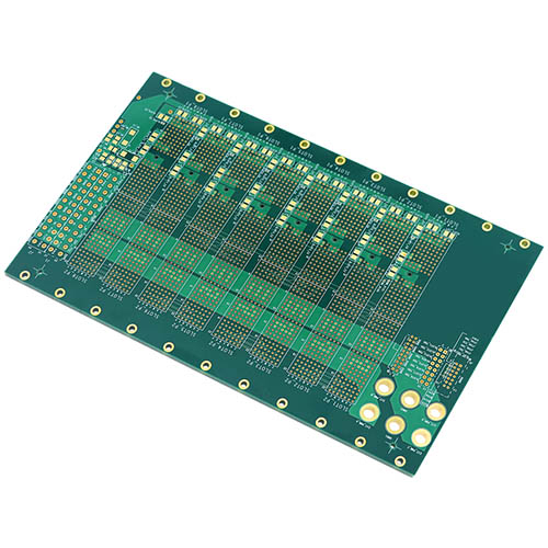
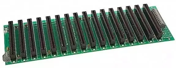
In today’s data-driven world, high-speed communication systems demand exceptional signal integrity, power stability, and system reliability. At the core of these systems lies the communication backplane PCB, which serves as the backbone for high-speed data transmission between multiple modules.
This case study highlights how KKPCB delivered a high-performance backplane PCB solution tailored for advanced telecommunication infrastructure, meeting strict requirements for high-speed signals, low loss, and reliability.
Project Background and Requirements
The client, a leading provider of communication equipment, required a multilayer backplane PCB capable of supporting:
- High-speed data rates (>25Gbps)
- Excellent signal integrity and low insertion loss
- Stable power distribution across multiple modules
- High layer count PCB design
- Long-term reliability in continuous operation
This project required advanced PCB design expertise and precise manufacturing capabilities.
Technical Challenges in Backplane PCB Design
1. Signal Integrity at High Data Rates
Maintaining signal integrity at high speeds is critical. Challenges included:
- Signal attenuation over long traces
- Crosstalk between high-speed channels
- Impedance mismatch
2. High Layer Count Complexity
The backplane PCB required a complex multilayer stack-up, increasing difficulty in:
- Layer alignment
- Manufacturing precision
- Thermal management
3. Power Integrity Requirements
Stable power delivery networks (PDN) were necessary to support multiple high-speed modules without noise interference.
4. Thermal Management
Continuous high-speed operation generates significant heat, requiring optimized heat dissipation design.
KKPCB Solution: Advanced Backplane PCB Design
1. Optimized Multilayer Stack-Up
KKPCB designed a high-performance multilayer PCB stack-up featuring:
- Dedicated signal, power, and ground layers
- Controlled impedance routing
- Reduced EMI and crosstalk
2. High-Speed Material Selection
To ensure low-loss performance, KKPCB selected advanced high-frequency PCB materials, offering:
- Low dielectric loss (Df)
- Stable dielectric constant (Dk)
- Excellent performance for high-speed signals
3. Signal Integrity Optimization
The design incorporated:
- Differential pair routing
- Back-drilling to reduce via stubs
- Careful trace length matching
These techniques significantly improved signal transmission quality.
4. Power Integrity Design
KKPCB optimized the power distribution network by:
- Using low-impedance power planes
- Strategic decoupling capacitor placement
- Minimizing power noise
5. Precision Manufacturing and Quality Control
To meet strict requirements, KKPCB applied:
- High-precision lamination processes
- Advanced drilling and plating technologies
- Comprehensive AOI, X-ray, and electrical testing
Results and Performance Outcomes
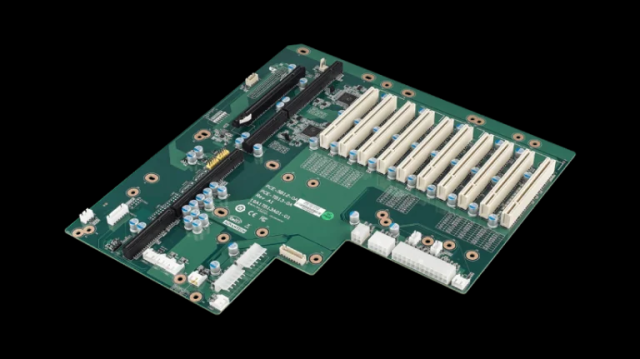
The final communication backplane PCB solution delivered:
- Excellent signal integrity at high data rates
- Reduced signal loss and crosstalk
- Stable power distribution
- Reliable performance under continuous operation
- High manufacturing consistency and yield
Applications in Communication Systems
This backplane PCB solution is widely applicable in:
- Telecommunication infrastructure
- Data centers and servers
- Network switches and routers
- Cloud computing systems
These applications require high-performance PCB solutions for reliable data transmission.
Key Takeaways from This Case Study
- Advanced PCB materials are essential for high-speed performance
- Proper stack-up design improves both signal and power integrity
- Precision manufacturing is critical for high-layer PCBs
- Collaboration with experienced PCB manufacturers ensures project success
Conclusion: Driving High-Speed Connectivity with KKPCB
This case study demonstrates how KKPCB successfully delivered a high-performance communication backplane PCB solution by combining advanced design techniques, high-quality materials, and precise manufacturing processes.
As demand for high-speed communication systems continues to grow, reliable backplane PCB solutions will remain a key factor in enabling next-generation connectivity.
