
Understanding RF PCB Design in Modern High-Frequency Electronics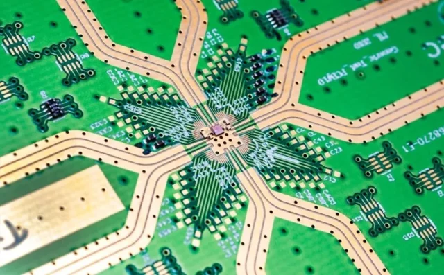
As wireless communication technology rapidly advances toward:
- 5G and 6G communication
- millimeter-wave systems
- satellite communication
- automotive radar
- IoT wireless networks
- aerospace RF systems
the importance of advanced RF PCB design has become increasingly critical.
Unlike conventional digital PCB systems, RF circuits in PCB design operate at:
- high frequencies
- extremely fast signal speeds
- sensitive electromagnetic conditions
At RF and microwave frequencies, even small PCB layout issues can significantly affect:
- signal integrity
- insertion loss
- impedance stability
- electromagnetic interference (EMI)
- RF transmission efficiency
Therefore, successful RF PCB engineering requires specialized knowledge of:
- RF interfaces
- controlled impedance PCB design
- transmission line theory
- grounding techniques
- electromagnetic behavior
- high-frequency PCB materials
This article explores the key characteristics of RF interfaces and RF circuits in PCB design, focusing on:
- RF signal behavior
- microwave PCB layout
- impedance control
- RF routing techniques
- EMI suppression
- high-frequency PCB reliability
What Is an RF Circuit in PCB Design?
An RF circuit is an electronic circuit designed to process:
- radio frequency signals
- microwave signals
- high-frequency electromagnetic waves
Typical RF frequency ranges include:
- MHz frequencies
- GHz frequencies
- millimeter-wave bands
RF circuits are widely used in:
- wireless communication devices
- radar systems
- satellite modules
- RF amplifiers
- RF transceivers
- wireless IoT equipment
Because RF signals are highly sensitive, RF PCB design must carefully control:
- signal loss
- impedance variation
- electromagnetic coupling
- transmission efficiency
What Are RF Interfaces?
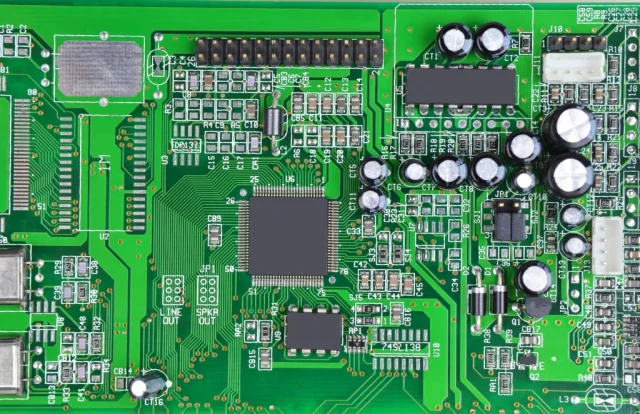
Definition of RF Interfaces
An RF interface is the connection point used for:
- RF signal transmission
- microwave signal input/output
- antenna connection
- RF module integration
RF interfaces may include:
- coaxial connectors
- SMA connectors
- MMCX connectors
- antenna feed structures
- RF test ports
The RF interface directly affects:
- signal integrity
- insertion loss
- return loss
- impedance matching
Key Characteristics of RF Circuits in PCB Design
1. High-Frequency Signal Sensitivity
One of the most important characteristics of RF PCB circuits is extreme sensitivity to:
- PCB layout variation
- trace geometry
- dielectric properties
- grounding quality
At high frequencies:
- PCB traces behave as transmission lines
- parasitic capacitance becomes significant
- inductive effects increase dramatically
Even small layout changes can cause:
- signal reflection
- insertion loss
- impedance mismatch
- phase instability
2. Controlled Impedance Requirement
Controlled impedance is essential in:
- RF PCB design
- microwave PCB layout
- antenna PCB systems
Typical RF impedance:
- 50-ohm impedance
- 75-ohm impedance
Controlled impedance depends on:
- trace width
- dielectric constant
- substrate thickness
- ground reference distance
Accurate impedance control improves:
- signal transmission efficiency
- RF power transfer
- measurement consistency
3. Transmission Line Behavior
At RF frequencies, PCB traces no longer behave as simple conductors.
Instead, they function as:
- microstrip transmission lines
- stripline structures
- coplanar waveguides
These structures must be carefully designed to minimize:
- signal attenuation
- reflection
- impedance discontinuity
4. Signal Integrity Challenges
RF circuits are highly vulnerable to:
- signal loss
- crosstalk
- EMI interference
- return loss
- phase distortion
Maintaining excellent RF signal integrity requires:
- optimized routing
- precise grounding
- low-loss PCB materials
5. Low-Loss PCB Material Requirement
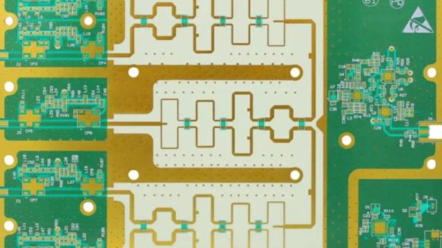
Standard FR4 PCB material may not perform well at:
- microwave frequencies
- millimeter-wave frequencies
Advanced RF PCB materials offer:
- low dielectric loss
- stable dielectric constant
- reduced insertion loss
Popular RF PCB materials include:
Characteristics of RF Interfaces in PCB Design
1. Impedance Matching Requirement
RF interfaces require precise:
- impedance matching
- transmission line continuity
Poor matching causes:
- return loss
- signal reflection
- RF efficiency reduction
Proper RF interface design improves:
- power transfer
- signal stability
- communication performance
2. Connector Transition Optimization
The transition between:
- RF connector
- PCB transmission line
must minimize:
- impedance discontinuity
- insertion loss
- parasitic inductance
Common RF connectors:
- SMA connectors
- SMP connectors
- coaxial interfaces
3. Grounding Around RF Interfaces
Proper grounding improves:
- EMI suppression
- RF shielding
- signal return stability
Ground via stitching is commonly used near:
- RF connectors
- antenna feed structures
- microwave interfaces
4. Shielding and Isolation
RF interfaces require strong isolation from:
- digital noise
- power switching circuits
- high-speed digital signals
Isolation techniques include:
- ground shielding
- RF isolation walls
- separated RF regions
RF PCB Routing Characteristics
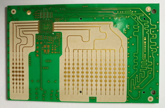
1. Short RF Routing Paths
Long RF traces increase:
- insertion loss
- radiation
- signal degradation
Best practice:
- keep RF routing as short as possible
2. Smooth Trace Geometry
Sharp corners create:
- impedance discontinuities
- signal reflection
Recommended routing:
- curved traces
- 45-degree routing
- smooth transitions
3. Consistent Reference Plane
RF transmission lines require:
- continuous ground reference
Ground plane interruptions may cause:
- EMI problems
- impedance instability
- RF radiation increase
4. Via Optimization in RF PCB Design
Vias can introduce:
- parasitic inductance
- signal reflection
- RF resonance
Optimization methods:
- minimize via count
- use back drilling
- apply ground via shielding
RF PCB Stack-Up Design Characteristics
Multilayer RF PCB Structures
RF PCB stack-up design often includes:
- dedicated RF signal layers
- continuous ground planes
- isolated power layers
Benefits:
- improved signal integrity
- EMI reduction
- controlled impedance stability
Power Integrity in RF PCB Design
RF systems require:
- ultra-clean power supply
- low-noise voltage regulation
Power noise can affect:
- phase noise
- RF sensitivity
- signal stability
Decoupling capacitors and filtering circuits are critical in:
- RF transceiver PCB design
- microwave amplifier systems
EMI and EMC Characteristics in RF PCB Design
RF circuits both:
- generate electromagnetic energy
and: - receive electromagnetic interference
Proper RF PCB design minimizes:
- radiated emissions
- coupling noise
- electromagnetic susceptibility
EMI control methods:
- shielding
- grounding
- trace spacing optimization
- filter implementation
Thermal Management in RF PCB Design
High-frequency RF systems generate heat through:
- RF power amplification
- conductor loss
- dielectric loss
Thermal management techniques:
- thermal vias
- copper balancing
- heat sinks
- metal-backed RF PCB structures
Applications of RF PCB Interfaces and RF Circuits
RF PCB technology is widely used in:
- 5G communication systems
- satellite communication modules
- automotive radar
- aerospace electronics
- military RF systems
- wireless IoT devices
- RF test equipment
- microwave transceivers
Future Trends in RF PCB Design
1. Millimeter-Wave PCB Technology
Supporting:
- 77 GHz radar
- 5G mmWave
- 6G communication
2. Ultra-Low-Loss RF Materials
Future laminates focus on:
- lower dielectric loss
- higher thermal stability
- improved dimensional consistency
3. Advanced Antenna Integration
Including:
- antenna-in-package (AiP)
- phased-array antennas
- embedded RF modules
4. AI-Driven RF PCB Optimization
Using:
- electromagnetic simulation
- automated RF routing
- intelligent impedance tuning
Conclusion
The characteristics of RF interfaces and RF circuits in PCB design differ significantly from standard digital PCB systems.
Successful RF PCB engineering requires careful optimization of:
- controlled impedance
- transmission line routing
- grounding strategy
- EMI suppression
- RF shielding
- low-loss PCB materials
- signal integrity
By properly designing:
- RF interfaces
- microwave transmission lines
- multilayer RF PCB stack-ups
- antenna feed structures
engineers can achieve:
- stable RF performance
- low insertion loss
- excellent signal integrity
- reliable high-frequency communication
As wireless technology continues evolving toward:
- higher frequency
- faster communication
- greater bandwidth
- advanced RF integration
the importance of advanced RF PCB design technology will continue growing rapidly.

