
With the continuous development of electronic products toward miniaturization, higher performance, and greater functional integration, traditional PCB technologies are facing increasing limitations in terms of wiring density and space utilization.
HDI (High Density Interconnect) PCB technology has become one of the most important advanced PCB solutions for modern electronic systems. By using microvias, fine lines, and high-density interconnection structures, HDI PCBs enable more complex circuits to be integrated into smaller board areas while maintaining reliable electrical performance.
HDI PCBs are widely used in:
- Smartphones and consumer electronics
- Wearable devices
- Automotive electronics
- Medical equipment
- Communication systems
- Semiconductor test equipment
- Industrial control systems
Compared with conventional multilayer PCBs, HDI technology provides significant advantages in:
- Higher wiring density
- Smaller PCB size
- Improved signal integrity
- Better electrical performance
- Greater design flexibility
1. What Is an HDI PCB?
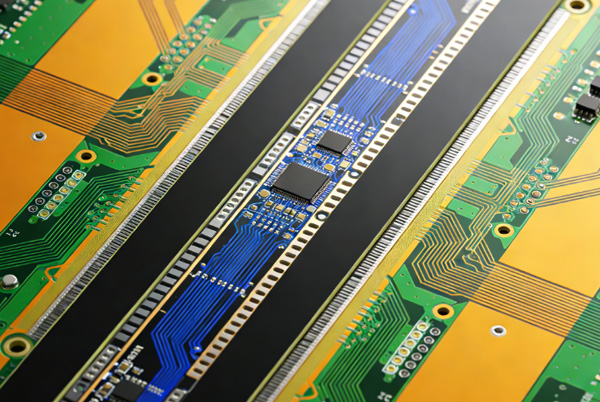
HDI (High Density Interconnect) PCB is an advanced circuit board technology that uses microvia interconnections and high-density routing structures to increase circuit integration.
Unlike traditional PCBs that mainly rely on mechanical through holes, HDI PCBs use:
- Laser-drilled microvias
- Blind vias
- Buried vias
- Fine-pitch wiring
to create shorter and more efficient electrical connections between layers.
The core idea of HDI technology is:
Achieve higher circuit density within a smaller PCB area through optimized interconnection structures.
2. Main Structures of HDI PCB
HDI PCBs can be classified according to their layer structure and manufacturing method.
2.1 1+N+1 HDI PCB
This is one of the most common HDI structures.
Structure:
- One HDI build-up layer on each side
- Conventional multilayer core in the center
Advantages:
- Lower manufacturing complexity
- Cost-effective
- Suitable for many compact electronic products
Applications:
- Consumer electronics
- Industrial controllers
- Portable devices
2.2 2+N+2 HDI PCB
This structure contains two HDI build-up layers on each side.
Advantages:
- Higher wiring density
- Better support for complex designs
Applications:
- High-performance computing
- Advanced communication equipment
- Automotive electronics
2.3 Any-Layer HDI PCB
Any-layer HDI allows microvias to connect between any layers.
Advantages:
- Maximum design flexibility
- Extremely high routing density
Applications:
- Advanced smartphones
- Semiconductor-related equipment
- High-end electronic systems
3. Key Technologies Used in HDI PCB Manufacturing
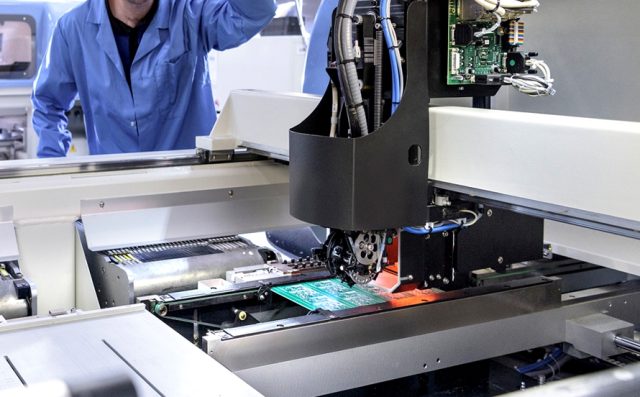
3.1 Microvia Technology
Microvias are small-diameter holes created by laser drilling.
Compared with traditional vias, microvias provide:
- Smaller size
- Higher density
- Shorter signal paths
Benefits include:
- More routing space
- Reduced PCB size
- Improved electrical performance
3.2 Laser Drilling Technology
Laser drilling is essential for HDI PCB production.
Advantages:
- High precision
- Small hole diameter
- Suitable for fine-pitch designs
Important process controls include:
- Laser energy
- Hole depth
- Material compatibility
Poor laser processing may result in:
- Incomplete via formation
- Poor copper plating
- Reliability issues
3.3 Via Filling Technology
Microvias often require filling to improve reliability.
Common filling materials:
- Electroplated copper
- Conductive materials
Benefits:
- Improved mechanical strength
- Better electrical connection
- Suitable for stacked via structures
3.4 Fine-Line Circuit Manufacturing
HDI PCBs require advanced imaging and etching technology to achieve:
- Narrow trace width
- Small spacing
- High registration accuracy
Fine-line capability directly affects:
- Component density
- Routing flexibility
4. Advantages of HDI PCBs
4.1 Higher Wiring Density
The primary advantage of HDI technology is increased circuit density.
Compared with conventional multilayer PCBs, HDI allows:
- More signal routes
- Smaller board dimensions
- More compact product designs
4.2 Miniaturization of Electronic Products
HDI technology helps reduce PCB size while maintaining functionality.
Applications include:
- Smartphones
- Smart watches
- Portable medical devices
Benefits:
- Smaller product size
- Lower weight
- Improved design flexibility
4.3 Improved Signal Integrity
Shorter interconnection paths reduce:
- Signal delay
- Parasitic effects
- Electromagnetic interference
HDI is especially beneficial for:
- High-speed digital circuits
- RF communication systems
4.4 Better Thermal and Electrical Performance
HDI structures can improve:
- Power distribution
- Grounding performance
- Heat dissipation paths
Proper stackup design helps optimize:
- Power integrity
- Signal integrity
4.5 Improved Component Integration
HDI supports advanced component packages such as:
- BGA
- CSP
- Fine-pitch IC packages
This makes it suitable for highly integrated electronic systems.
5. HDI PCB Manufacturing Process
5.1 Engineering Review and DFM Analysis
Before manufacturing, engineers evaluate:
DFM analysis focuses on:
- Minimum trace width
- Via reliability
- Manufacturing feasibility
5.2 Inner Layer Fabrication
For multilayer HDI PCBs:
- Inner circuits are formed
- Copper patterns are created
- Layers are inspected
Accuracy is critical for layer alignment.
5.3 Lamination Process
Multiple PCB layers are laminated under controlled conditions.
Important parameters:
- Temperature
- Pressure
- Time
Poor lamination may cause:
- Delamination
- Layer shifting
- Reliability problems
5.4 Laser Via Formation
Laser drilling creates microvias between specific layers.
Key requirements:
- Accurate positioning
- Stable hole quality
- Proper aspect ratio
5.5 Copper Plating and Via Filling
After drilling:
- Hole walls are plated with copper
- Microvias are filled if required
This ensures reliable electrical connection.
5.6 Circuit Pattern Formation
Fine circuits are created through:
- Imaging
- Etching
- Inspection
Advanced equipment is required to maintain precision.
5.7 Surface Finishing
Common HDI PCB surface finishes include:
ENIG
Advantages:
- Flat surface
- Suitable for fine-pitch components
ENEPIG
Advantages:
- Higher reliability
- Suitable for advanced packaging
Immersion Silver
Advantages:
- Good electrical performance
- Suitable for high-frequency applications
6. HDI PCB Design Guidelines
6.1 Optimize Stackup Design
A suitable stackup should consider:
- Signal layers
- Ground planes
- Power layers
- Impedance requirements
Good stackup design improves:
- Signal integrity
- EMI performance
- Manufacturing reliability
6.2 Maintain Via Reliability
Important considerations:
- Microvia diameter
- Via depth
- Copper plating thickness
- Via spacing
Poor via design may cause:
- Via cracking
- Open circuits
6.3 Consider Signal Integrity
High-speed HDI designs should control:
- Impedance
- Crosstalk
- Signal return paths
Methods include:
- Controlled impedance routing
- Reference plane optimization
- Short signal paths
6.4 Apply DFM Principles
Early manufacturing review helps avoid:
- Excessive design complexity
- Production yield reduction
- Cost increases
7. Applications of HDI PCBs
7.1 Consumer Electronics
Applications:
- Smartphones
- Tablets
- Smart wearable devices
Requirements:
- Thin structure
- High integration density
7.2 Automotive Electronics
Applications:
- ADAS systems
- Vehicle controllers
- Sensor modules
Requirements:
- High reliability
- Thermal stability
- Long service life
7.3 Medical Electronics
Applications:
- Portable monitoring devices
- Diagnostic equipment
Requirements:
- Compact design
- Stable electrical performance
7.4 Communication Systems
Applications:
- 5G equipment
- Network devices
- RF modules
Requirements:
- High-speed signal transmission
- Low signal loss
7.5 Semiconductor Test Equipment
Applications:
- ATE load boards
- Test interface boards
Requirements:
- Fine-pitch connections
- High-speed signal integrity
- High reliability
8. Challenges in HDI PCB Manufacturing
8.1 Higher Manufacturing Complexity
HDI production requires:
- Advanced equipment
- Precise process control
- Experienced engineering teams
8.2 Higher Cost
Compared with standard PCBs, HDI PCBs involve:
- More manufacturing steps
- More inspection requirements
- Higher material costs
8.3 Reliability Control
Important reliability factors include:
- Microvia strength
- Copper plating quality
- Lamination consistency
9. Future Development Trends of HDI PCB Technology
Higher Density Interconnection
Future HDI development will focus on:
- Smaller microvias
- Finer lines
- More advanced structures
Integration with Advanced Packaging
HDI technology will continue supporting:
- Semiconductor packages
- High-performance computing
- AI hardware systems
Improved Reliability and Manufacturing Efficiency
Future improvements will focus on:
- Better materials
- Automated inspection
- Advanced process control
Conclusion
HDI PCB technology is a key solution for modern electronic products requiring high integration density, compact design, and reliable electrical performance.
Through technologies such as:
- Microvias
- Laser drilling
- Fine-line routing
- Advanced stackup design
- Controlled impedance manufacturing
HDI PCBs enable manufacturers to achieve smaller, faster, and more reliable electronic systems.
As applications continue evolving toward higher speeds and greater miniaturization, HDI PCB technology will remain an essential foundation for next-generation electronics.
