
With the continuous development of electronic products toward higher performance, smaller size, and greater functional integration, traditional single-layer and double-layer PCBs can no longer satisfy the requirements of many advanced applications.
A multilayer PCB is a circuit board composed of multiple conductive copper layers laminated together with insulating dielectric materials. By increasing the number of layers, designers can achieve higher routing density, better electrical performance, and improved reliability for complex electronic systems.
Today, multilayer PCBs are widely used in:
- Communication equipment
- Industrial control systems
- Automotive electronics
- Medical devices
- Aerospace electronics
- High-speed computing systems
However, while multilayer PCBs provide significant advantages, they also introduce challenges related to design complexity, manufacturing difficulty, and cost.
Understanding the advantages and disadvantages of multilayer PCBs helps engineers select the most suitable PCB structure for their applications.
1. What Is a Multilayer PCB?
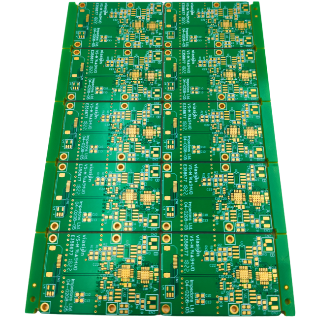
A multilayer PCB consists of three or more copper layers combined through lamination processes.
A typical multilayer PCB structure includes:
- Top signal layer
- Internal signal layers
- Ground planes
- Power planes
- Bottom signal layer
- Prepreg and core dielectric materials
Common multilayer PCB configurations include:
- 4-layer PCB
- 6-layer PCB
- 8-layer PCB
- 10-layer PCB
- 12-layer and higher-layer PCB
Each layer can be assigned different functions to optimize:
- Signal routing
- Power distribution
- EMI control
- Thermal management
2. Advantages of Multilayer PCBs
2.1 Higher Wiring Density
One of the biggest advantages of multilayer PCBs is their ability to provide more routing space.
Compared with single-layer or double-layer boards, multilayer structures allow designers to:
- Add more signal paths
- Reduce trace congestion
- Support complex circuits
Additional internal layers create more design flexibility, especially for products requiring many components in limited space.
Applications include:
- Smartphones
- Network equipment
- Embedded systems
- Industrial controllers
2.2 Smaller PCB Size and Weight
Multilayer PCBs allow more circuits to be integrated into a smaller board area.
Instead of increasing PCB dimensions, engineers can add internal layers to accommodate additional connections.
Benefits include:
- Compact product design
- Reduced system weight
- Improved space utilization
This is especially important for:
- Portable electronics
- Wearable devices
- Aerospace equipment
2.3 Improved Signal Integrity
High-speed electronic systems require stable signal transmission.
Multilayer PCBs provide dedicated layers for:
- Signal routing
- Ground reference
- Power distribution
This helps improve:
- Signal return paths
- Impedance control
- Noise reduction
For high-speed applications, proper multilayer stack-up design can reduce:
- Signal reflection
- Crosstalk
- Electromagnetic interference
2.4 Better Power Distribution
Dedicated power and ground planes are major advantages of multilayer PCB structures.
Benefits include:
- Lower power distribution impedance
- More stable voltage delivery
- Reduced power noise
This is important for:
- Processors
- High-speed ICs
- Communication modules
2.5 Enhanced EMI and EMC Performance
Electromagnetic compatibility is a major concern in modern electronics.
Multilayer PCBs help control electromagnetic interference by:
- Using internal ground planes
- Reducing current loop areas
- Providing shielding effects
Proper stack-up design improves:
- Noise suppression
- Signal stability
- EMC compliance
2.6 Improved Mechanical Strength
The laminated structure of multilayer PCBs provides better mechanical rigidity compared with simple PCB structures.
Advantages include:
- Better dimensional stability
- Higher structural strength
- Improved reliability in demanding environments
2.7 Support for Advanced PCB Technologies
Multilayer PCBs can integrate advanced technologies such as:
- HDI (High Density Interconnect)
- Microvias
- Blind vias
- Buried vias
- Controlled impedance routing
These technologies enable the development of high-performance electronic products.
3. Disadvantages of Multilayer PCBs
3.1 Higher Manufacturing Cost
The manufacturing process of multilayer PCBs is more complex than standard PCBs.
Additional processes include:
- Multiple lamination cycles
- Internal layer fabrication
- Layer alignment
- Advanced inspection
As a result, multilayer PCBs generally have higher production costs.
Cost factors include:
- Number of layers
- Material selection
- Manufacturing requirements
- Surface finish
3.2 More Complex PCB Design
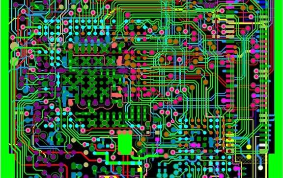
Designing multilayer PCBs requires advanced engineering knowledge.
Engineers must carefully consider:
- Layer arrangement
- Signal integrity
- Power distribution
- Impedance control
- Thermal management
Poor stack-up design may result in:
- Signal quality problems
- EMI issues
- Manufacturing difficulties
3.3 Longer Manufacturing Lead Time
Compared with simple PCBs, multilayer PCBs require more manufacturing steps.
Additional processes include:
- Inner layer imaging
- Layer lamination
- Drilling
- Plating
- Electrical testing
This increases production time, especially for:
- High-layer-count boards
- HDI PCBs
- Prototype builds
3.4 More Difficult Repair and Modification
Because multilayer PCBs contain internal layers, troubleshooting can be more difficult.
Challenges include:
- Limited access to internal connections
- Difficulty identifying faults
- More complicated repair processes
Compared with single-layer PCBs, modifications are more challenging.
3.5 Higher Requirements for Manufacturing Capability
Multilayer PCB production requires strict process control.
Important manufacturing capabilities include:
- Precise layer alignment
- Controlled lamination
- Advanced drilling technology
- Reliable plating processes
Manufacturing defects may include:
- Layer misalignment
- Delamination
- Via failure
- Impedance deviation
3.6 Increased Risk of Thermal Problems
Higher component density can create thermal challenges.
Potential issues include:
- Heat accumulation
- Uneven temperature distribution
- Reduced component lifetime
Engineers need to consider:
- Copper planes
- Thermal vias
- Heat dissipation paths
4. Multilayer PCB Stack-Up Design Considerations
4.1 Layer Function Planning
Each PCB layer should have a clear purpose.
Typical allocation:
Signal Layers
Used for:
- High-speed routing
- Component connections
Ground Layers
Used for:
- Signal return paths
- EMI reduction
Power Layers
Used for:
- Stable power distribution
4.2 Balanced Stack-Up Design
A balanced stack-up helps reduce:
- PCB warpage
- Mechanical stress
- Manufacturing variation
Important factors include:
- Symmetrical copper distribution
- Consistent dielectric thickness
- Proper material selection
4.3 Impedance Control
For high-speed multilayer PCBs, impedance control is essential.
Factors affecting impedance include:
- Trace width
- Copper thickness
- Dielectric thickness
- Material dielectric constant
Common requirements:
- 50Ω single-ended impedance
- 90Ω/100Ω differential impedance
5. Applications of Multilayer PCBs
Communication Equipment
Examples:
- Routers
- Base stations
- RF communication systems
Requirements:
- High-speed transmission
- EMI control
Automotive Electronics
Examples:
- ADAS systems
- Vehicle control modules
- Radar systems
Requirements:
- High reliability
- Environmental resistance
Industrial Control Systems
Examples:
- PLC controllers
- Automation equipment
Requirements:
- Stable operation
- Long service life
Medical Electronics
Examples:
- Monitoring devices
- Diagnostic equipment
Requirements:
- High reliability
- Signal accuracy
Aerospace Electronics
Requirements:
- Lightweight design
- High reliability
- Extreme environment operation
6. Multilayer PCB Manufacturing Considerations
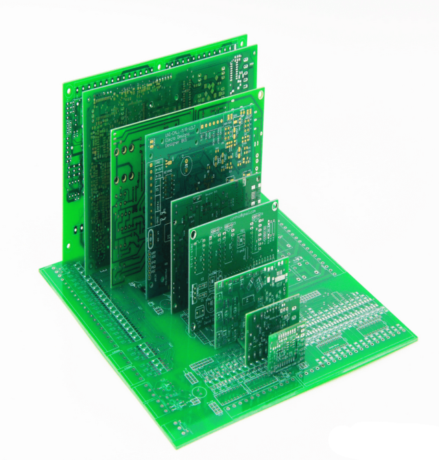
6.1 Material Selection
Common materials include:
- Standard FR-4
- High-Tg FR-4
- Low-loss materials
- Rogers laminates
Selection depends on:
- Frequency requirements
- Thermal conditions
- Reliability requirements
6.2 Lamination Process Control
Lamination quality directly affects PCB reliability.
Important parameters:
- Temperature
- Pressure
- Material compatibility
- Curing process
6.3 Inspection and Testing
Common quality controls include:
- AOI inspection
- X-ray inspection
- Electrical testing
- Impedance testing
These processes help ensure:
- Layer connection reliability
- Signal performance
- Manufacturing consistency
7. How to Choose a Multilayer PCB?
A multilayer PCB is suitable when the product requires:
- High circuit density
- Complex routing
- High-speed signal transmission
- Reliable power distribution
- EMI control
However, engineers should evaluate:
- Product cost
- Manufacturing capability
- Production volume
- Performance requirements
For simple circuits, fewer-layer PCBs may provide a more economical solution.
Conclusion
Multilayer PCBs provide significant advantages for modern electronic systems, including higher wiring density, improved signal integrity, better power distribution, and enhanced reliability.
However, they also introduce challenges such as:
- Higher manufacturing cost
- Increased design complexity
- Longer production cycles
- More demanding fabrication requirements
A successful multilayer PCB solution requires careful coordination between:
- PCB designers
- Manufacturing engineers
- Material suppliers
- Assembly teams
By optimizing stack-up design, material selection, and manufacturing processes, multilayer PCBs can provide reliable performance for increasingly complex electronic applications.
