
With the increasing demand for higher frequency communication, advanced radar systems, and high-speed electronic applications, PCB materials must provide stable electrical performance while maintaining reliable manufacturability.
RO4003C™, RO4350B™, and RO4835™ laminates are high-frequency circuit materials developed for applications requiring low signal loss, stable dielectric properties, and improved thermal performance. These materials combine ceramic-filled hydrocarbon resin technology with glass reinforcement, providing RF performance advantages while remaining compatible with many conventional PCB manufacturing processes.
They are commonly used in:
- RF communication systems
- Microwave circuits
- 5G infrastructure
- Automotive radar
- Aerospace electronics
- High-speed digital systems
- Power amplifiers
However, compared with standard FR-4 materials, high-frequency laminates require more controlled processing methods during PCB fabrication to maintain electrical performance and reliability.
This article provides a quick reference guide covering key manufacturing considerations for RO4003C, RO4350B, and RO4835 laminates.
1. Material Overview of RO4003C, RO4350B, and RO4835
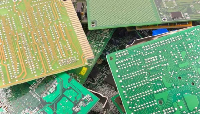
RO4003C, RO4350B, and RO4835 are ceramic-filled hydrocarbon resin composite laminates designed for high-frequency circuit applications. They offer stable electrical properties, low dielectric loss, and compatibility with multilayer PCB manufacturing processes.
RO4003C
RO4003C is designed for cost-effective high-frequency PCB applications requiring:
- Low dielectric loss
- Stable dielectric constant
- Reliable impedance control
- Compatibility with standard PCB processing
Typical applications include:
- RF circuits
- Wireless communication equipment
- Power amplifiers
- Microwave modules
RO4350B
RO4350B provides a balance between RF performance and manufacturing flexibility.
Key advantages include:
- Low-loss signal transmission
- Stable electrical performance
- Good thermal reliability
- Compatibility with standard PCB fabrication processes
It is widely used in:
- Base station equipment
- Automotive radar systems
- High-frequency amplifiers
- RF modules
RO4835
RO4835 is designed for demanding high-frequency applications requiring improved environmental and thermal stability.
Typical applications include:
- Microwave systems
- Advanced communication equipment
- Aerospace electronics
- High-reliability RF products
2. Storage Requirements Before Processing
Proper material storage is important to maintain laminate performance.
Recommended storage conditions include:
- Room temperature environment
- Dry and clean storage area
- Protection from contamination and moisture
A material tracking system based on laminate lot numbers is recommended to support manufacturing traceability and quality control.
3. Inner Layer Preparation
Proper inner layer preparation directly affects multilayer PCB reliability.
Tooling Requirements
RO4003C, RO4350B, and RO4835 laminates are compatible with various tooling systems, including:
- Round pin systems
- Slotted pin systems
- Pinned and pinless tooling methods
The tooling method should be selected according to:
- PCB layer count
- Registration requirements
- Manufacturing capability
Copper Surface Preparation
Before imaging and etching, copper surfaces require proper preparation.
Depending on laminate thickness, manufacturers may use:
Chemical Preparation
Suitable for thinner cores.
Typical processes include:
- Cleaning
- Micro-etching
- Rinsing
- Drying
Mechanical Preparation
More suitable for thicker cores where controlled surface treatment is required.
Photoresist and DES Processing
RO4003C, RO4350B, and RO4835 materials support standard PCB processes, including:
- Film photoresist
- Liquid photoresist
- Develop
- Etch
- Strip (DES)
Thin cores may require additional handling methods to maintain process stability.
4. Multilayer Bonding Considerations
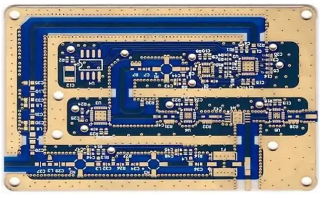
Multilayer PCB fabrication requires careful control of bonding processes.
Pre-Baking Before Lamination
A pre-bake process is recommended before bonding.
Typical temperature range:
125°C–150°C (257°F–302°F)
This helps reduce moisture-related risks during multilayer processing.
Bonding Materials
RO4003C, RO4350B, and RO4835 laminates are compatible with:
- RO4400™ series bondplies
- Various thermoset prepreg systems
The specific bonding cycle should follow the parameters recommended for the selected adhesive system.
5. Drilling Process Considerations
Drilling quality is critical because via reliability directly affects RF PCB performance.
Important drilling factors include:
- Drill speed
- Feed rate
- Tool wear
- Hole quality
Recommended Practices
During drilling:
- Use suitable entry and exit materials
- Control drilling parameters
- Monitor drill wear
- Maintain proper chip removal
Standard drill geometries are generally preferred because they provide better debris evacuation during drilling.
Hole Preparation
After drilling, manufacturers may use:
- Chemical desmear
- Plasma desmear
to improve hole wall preparation before metallization.
Aggressive etchback processes are generally not recommended for these materials.
6. Metallization and Plating
Reliable via metallization is essential for high-frequency multilayer PCBs.
Common processes include:
- Electroless copper deposition
- Direct metallization processes
Proper plating ensures:
- Reliable electrical connections
- Stable RF performance
- Improved mechanical reliability
7. Outer Layer Processing
RO4003C, RO4350B, and RO4835 laminates are compatible with common PCB finishing processes.
Supported surface finishes include:
- ENIG
- ENEPIG
- OSP
- Other standard final finishes
Before applying solder mask, proper surface preparation and baking processes are recommended to maintain reliability.
8. Routing and Mechanical Processing
These laminates can be processed through:
- CNC routing
- Punching
- V-scoring
Recommended routing practices include:
- Using diamond-cut router tools
- Applying suitable chipbreaker router bits
- Controlling mechanical stress
For V-scoring, excessive cutting depth should be avoided because it may cause premature board separation.
9. PCB Design Considerations for RO4003C/RO4350B/RO4835
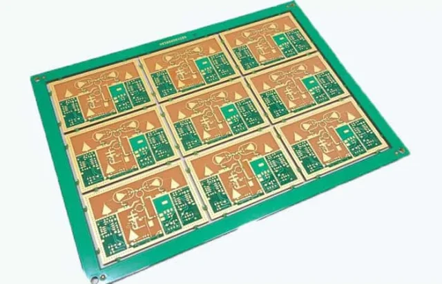
Material selection alone does not guarantee RF performance. PCB design must also consider:
Controlled Impedance
High-frequency circuits require accurate impedance control.
Important parameters include:
- Dielectric thickness
- Copper thickness
- Trace width
- Material Dk value
Stack-Up Optimization
A suitable stack-up helps maintain:
- Stable transmission characteristics
- Reduced signal loss
- Improved EMI performance
RF Trace Design
High-frequency routing should consider:
- Short signal paths
- Continuous reference planes
- Proper grounding
- Reduced discontinuities
10. Applications of RO4003C/RO4350B/RO4835 PCBs
These laminates are widely used in advanced electronic systems, including:
Communication Systems
- 5G base stations
- RF modules
- Wireless communication equipment
Automotive Electronics
- 24 GHz radar
- 77 GHz radar systems
- Vehicle communication systems
Aerospace and Defense
- Microwave systems
- Satellite communication
- High-reliability electronics
Industrial Applications
- Sensor systems
- Test equipment
- High-speed control systems
Conclusion
RO4003C, RO4350B, and RO4835 laminates provide excellent solutions for high-frequency and high-speed PCB applications where electrical stability and manufacturing reliability are critical.
Successful processing requires careful control of:
- Material storage and preparation
- Inner layer processing
- Multilayer bonding
- Drilling and metallization
- Final circuit fabrication
By combining appropriate material selection, optimized PCB design, and controlled manufacturing processes, engineers can achieve reliable RF performance, stable impedance characteristics, and long-term product reliability.
For high-frequency PCB projects, close cooperation between PCB designers and manufacturers is essential to ensure that material advantages are fully realized in the final product.
