
Electrostatic discharge (ESD) is one of the most common reliability challenges in modern electronic products. With increasing levels of integration, smaller component packages, and faster signal transmission speeds, electronic devices have become more sensitive to transient electrical disturbances.
ESD events can occur during:
- Product assembly
- Transportation
- User operation
- Maintenance activities
- External cable connection
A sudden electrostatic discharge may generate extremely high voltage pulses within a very short time, potentially causing:
- Semiconductor damage
- Data corruption
- System malfunction
- Permanent circuit failure
Therefore, ESD prevention must be considered during PCB design, rather than being added only after product testing failures occur.
A reliable PCB ESD protection strategy combines:
- Circuit protection components
- Proper grounding design
- PCB layout optimization
- Signal routing control
- Mechanical and system-level protection
This article explains the key principles and practical methods for improving ESD resistance in PCB design.
1. Understanding ESD and Its Impact on PCB Systems
1.1 What Is ESD?
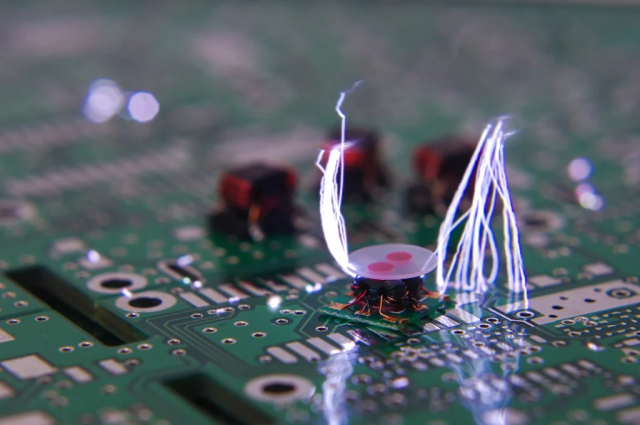
Electrostatic discharge is the rapid transfer of electrical charge between objects with different electrical potentials.
Common sources include:
The discharge process produces:
- High voltage
- High current pulses
- Fast transient energy
Although the duration is extremely short, the peak energy can damage sensitive electronic components.
2. Why PCB Designs Need ESD Protection
Modern PCBs contain many sensitive devices, including:
- Microcontrollers
- Communication ICs
- Sensors
- Memory devices
- RF modules
- Power management chips
ESD events may cause:
2.1 Permanent Damage
Examples:
- Semiconductor junction breakdown
- IC internal damage
- Burned components
2.2 Temporary Malfunctions
Examples:
- System reset
- Communication interruption
- Incorrect data processing
2.3 Reduced Product Reliability
Repeated ESD stress may weaken components and shorten product lifetime.
3. Main ESD Protection Methods in PCB Design
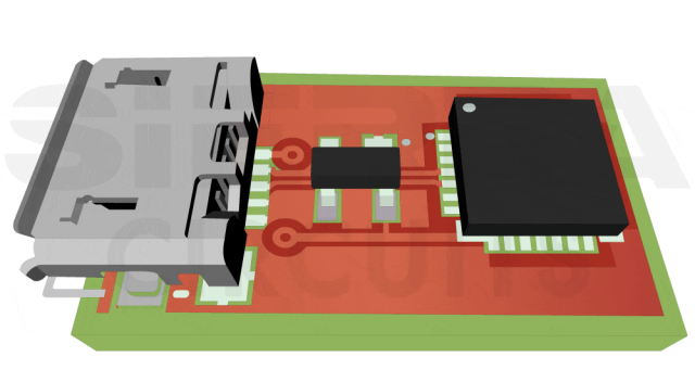
3.1 Use ESD Protection Devices
The first protection layer is usually placed near external interfaces.
Common protection components include:
TVS (Transient Voltage Suppression) Diodes
TVS diodes are widely used for ESD protection.
Functions:
- Clamp transient voltage
- Absorb surge energy
- Protect sensitive ICs
Applications:
- USB interfaces
- Ethernet ports
- Communication connectors
ESD Protection ICs
Dedicated ESD protection devices provide:
- Low capacitance
- Fast response
- High protection performance
Suitable for:
- High-speed data interfaces
- Sensitive communication circuits
4. Proper Placement of ESD Protection Components
The location of protection components directly affects effectiveness.
Recommended Placement
ESD protection devices should be placed:
- Close to external connectors
- Before sensitive circuits
- With short discharge paths
Example:
Incorrect:
Connector → Long Trace → TVS → IC
Correct:
Connector → TVS → IC
A shorter protection path reduces:
- Parasitic inductance
- Residual voltage
- Protection response time
5. Grounding Design for ESD Protection
Grounding is one of the most important aspects of ESD-resistant PCB design.
A good grounding structure provides:
- Low impedance discharge paths
- Controlled current flow
- Reduced interference
5.1 Use a Solid Ground Plane
A continuous ground plane helps:
- Spread ESD energy
- Reduce voltage rise
- Improve return current paths
Avoid unnecessary ground interruptions.
5.2 Provide Short Ground Connections
The connection between ESD protection devices and ground should be:
- Short
- Wide
- Direct
Long narrow ground traces increase inductance and reduce protection effectiveness.
5.3 Separate Sensitive Ground Areas Properly
For mixed-signal PCBs:
- Analog circuits
- Digital circuits
- Power circuits
should be carefully arranged.
However, excessive ground splitting may create:
- High impedance paths
- Uncontrolled ESD currents
The design should focus on maintaining proper return paths.
6. PCB Layout Techniques for ESD Protection
6.1 Keep ESD Paths Away from Sensitive Circuits
ESD current should have a controlled route.
Avoid routing ESD discharge paths near:
- Clock signals
- Reset lines
- Analog sensor traces
- RF circuits
6.2 Increase Clearance Around Sensitive Signals
Adequate spacing reduces:
- Capacitive coupling
- Spark-over risk
- Noise injection
6.3 Use Guard Traces
Grounded guard traces can provide additional protection.
Benefits:
- Reduce electromagnetic coupling
- Shield sensitive signals
- Improve noise immunity
Applications:
- Sensor circuits
- High-impedance analog signals
6.4 Optimize Via Design
Vias affect ESD current paths.
Good practices:
- Use multiple vias for high-current discharge paths
- Avoid long via transitions
- Connect protection devices directly to ground planes
7. ESD Protection for Different PCB Interfaces
7.1 USB Interface Protection
USB ports are frequently exposed to external contact.
Important considerations:
- Place TVS devices near connector
- Maintain differential pair impedance
- Minimize parasitic capacitance
7.2 Ethernet Interface Protection
Protection design should consider:
- Surge protection
- Transformer isolation
- Signal integrity
7.3 Sensor Interfaces
Sensor circuits are highly sensitive.
Recommended methods:
- Filtering circuits
- ESD diodes
- Short signal paths
- Proper grounding
7.4 RF Interfaces
RF circuits require special attention because additional protection components may introduce:
- Parasitic capacitance
- Signal loss
- Impedance changes
Design must balance:
- ESD protection
- RF performance
8. ESD Protection in Multilayer PCB Design
Multilayer PCBs provide additional design flexibility.
Recommended structures include:
Dedicated Ground Layers
Advantages:
- Lower impedance
- Better discharge capability
Controlled Signal Layer Arrangement
High-speed signals should be placed near:
- Continuous reference planes
Benefits:
- Reduced noise coupling
- Better EMI performance
Power Plane Optimization
Proper power distribution helps prevent:
- Voltage fluctuation
- System instability
9. Material and Manufacturing Considerations
ESD performance is also influenced by PCB manufacturing quality.
9.1 PCB Material Selection
Material properties affect:
- Insulation performance
- Moisture resistance
- Reliability
Common choices:
- FR-4
- High-Tg FR-4
- Specialized high-reliability laminates
9.2 Surface Finish
Surface finishes such as:
- ENIG
- ENEPIG
provide:
- Good conductivity
- Corrosion resistance
- Reliable contact performance
9.3 PCB Cleanliness
Contaminants may reduce insulation resistance.
Manufacturing control should include:
- Cleaning processes
- Ionic contamination control
- Inspection procedures
10. Common ESD Design Mistakes
10.1 Placing Protection Devices Too Far from Connectors
Problem:
Long ESD current path.
Result:
Reduced protection effectiveness.
10.2 Sharing ESD Current Paths with Sensitive Signals
Problem:
ESD noise enters critical circuits.
Result:
System malfunction.
10.3 Ignoring Parasitic Inductance
Problem:
Protection components cannot respond effectively.
Result:
Higher residual voltage.
10.4 Overusing Ground Splitting
Problem:
Creates poor discharge paths.
Result:
Uncontrolled ESD current flow.
11. ESD Testing and Verification
After PCB design, ESD performance should be verified.
Common standards include:
- IEC 61000-4-2
- ISO 10605 (automotive applications)
Testing evaluates:
- Contact discharge
- Air discharge
- System recovery behavior
Testing Methods
System-Level ESD Testing
Evaluates:
- Complete product immunity
- Functional stability
Component-Level Testing
Evaluates:
- Device protection capability
12. Practical ESD Design Workflow
A reliable ESD protection process includes:
Step 1: Identify Exposure Points
Analyze:
- External connectors
- User-accessible areas
- Cable interfaces
Step 2: Select Protection Components
Consider:
- Voltage rating
- Clamping voltage
- Capacitance
Step 3: Design PCB Protection Layout
Optimize:
- Component placement
- Ground paths
- Signal routing
Step 4: Perform Simulation and Testing
Verify:
- Protection effectiveness
- Signal integrity
- System reliability
Conclusion
ESD prevention is an essential part of modern PCB design. As electronic products become smaller, faster, and more integrated, effective ESD protection becomes increasingly important.
A reliable ESD-resistant PCB design should combine:
- Proper protection components
- Optimized grounding
- Short discharge paths
- Careful signal routing
- Manufacturing quality control
By considering ESD protection from the early design stage, engineers can significantly improve product reliability, reduce field failures, and ensure stable operation in real-world environments.
