
With the increasing integration and miniaturization of electronic products, PCB designs are becoming more sensitive to external electrical disturbances. Among various reliability challenges, Electrostatic Discharge (ESD) is one of the most common threats that can affect electronic system performance and product lifetime.
Static electricity generated during human contact, manufacturing processes, transportation, or environmental changes can introduce high-voltage transient pulses into electronic circuits. Without effective protection, ESD events may cause:
- Component damage
- System malfunction
- Communication failures
- Reduced product reliability
Therefore, enhancing anti-static ESD protection during PCB design is essential for improving product robustness and ensuring compliance with industry reliability requirements.
1. Understanding the Impact of ESD on PCB Systems
Electrostatic discharge is a sudden transfer of electrical energy between objects with different electrical potentials.
Although ESD events usually occur within a very short duration, the transient voltage can reach several thousand volts.
Potential effects on electronic systems include:
Permanent Damage
High-voltage pulses may damage sensitive semiconductor components such as:
- Microcontrollers
- Sensors
- Communication ICs
- Memory devices
This damage may immediately cause product failure.
Latent Damage
In some cases, ESD does not completely destroy components but weakens internal structures.
This may result in:
- Reduced component lifetime
- Intermittent failures
- Field reliability issues
Functional Disturbance
ESD events may also cause temporary system problems, including:
- Unexpected resets
- Data corruption
- Communication interruption
2. PCB Layout Principles for ESD Protection
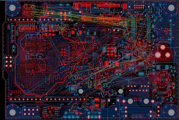
Effective ESD protection starts with proper PCB layout planning.
2.1 Minimize ESD Current Paths
When ESD enters a PCB through external interfaces, the discharge current should be guided away from sensitive circuits.
Design principles include:
- Keep ESD protection devices close to connectors
- Provide short discharge paths
- Avoid routing ESD current through sensitive areas
A shorter current path reduces the possibility of interference spreading throughout the PCB.
2.2 Place Protection Components Near Interfaces
External interfaces are common entry points for ESD.
Protection components should be placed close to:
- USB connectors
- Communication ports
- Power input terminals
- External sensor interfaces
Common protection devices include:
- TVS diodes
- ESD suppressors
- Surge protection components
The closer the protection device is to the entry point, the more effectively it can clamp transient voltage.
2.3 Maintain Proper Grounding Structure
Ground design directly affects ESD performance.
A reliable grounding structure helps:
- Provide a low-impedance discharge path
- Reduce voltage spikes
- Prevent noise coupling
Recommended practices include:
- Using continuous ground planes
- Adding sufficient ground vias
- Avoiding unnecessary ground discontinuities
3. ESD Protection Circuit Design Methods
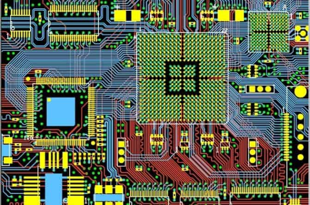
3.1 TVS Diode Protection
Transient Voltage Suppression (TVS) diodes are commonly used for ESD protection.
Their functions include:
- Clamping high-voltage pulses
- Protecting sensitive components
- Diverting transient current
Selection considerations include:
- Working voltage
- Clamping voltage
- Response time
- Capacitance characteristics
3.2 Series Resistor Protection
Series resistors can limit transient current and reduce stress on sensitive components.
They are commonly applied in:
- Signal lines
- Communication interfaces
- Control signals
However, resistance values must be carefully selected to avoid affecting signal quality.
3.3 Filter and Isolation Design
Additional protection methods include:
- Common-mode chokes
- Ferrite beads
- RC filters
- Signal isolation components
These methods help reduce high-frequency noise caused by ESD events.
4. ESD Considerations for High-Speed PCB Design
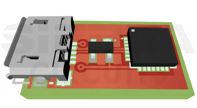
High-speed circuits require special attention because protection components may introduce parasitic effects.
Potential issues include:
- Increased capacitance
- Signal attenuation
- Impedance variation
For high-speed interfaces such as:
- USB
- Ethernet
- HDMI
- High-speed differential signals
designers should consider:
- Low-capacitance ESD devices
- Controlled impedance routing
- Differential pair matching
The protection strategy must balance ESD performance and signal integrity.
5. ESD Protection for Different PCB Applications
Consumer Electronics
Portable devices frequently face human contact and require strong ESD protection.
Common areas include:
- Buttons
- Charging ports
- Display interfaces
Industrial Control Systems
Industrial environments may contain stronger static interference sources.
Important considerations include:
- External communication interfaces
- Long cable connections
- Harsh operating conditions
Additional protection may be required for reliable operation.
Automotive Electronics
Automotive PCB systems must withstand:
- Temperature changes
- Electrical disturbances
- External transient events
ESD design is especially important for:
- Sensors
- Control modules
- Communication networks
6. Common ESD Design Mistakes
6.1 Placing Protection Devices Too Far from Connectors
A long trace between the connector and protection device increases inductance.
This may reduce protection effectiveness.
6.2 Sharing ESD Current Paths with Sensitive Circuits
If discharge current flows through sensitive areas, it may cause:
- System resets
- Signal errors
- Component damage
6.3 Ignoring PCB Stack-Up Effects
The layer structure affects ESD current return paths.
A well-designed multilayer PCB should provide:
- Stable reference planes
- Short grounding paths
- Good current distribution
7. Manufacturing Considerations for ESD Reliability
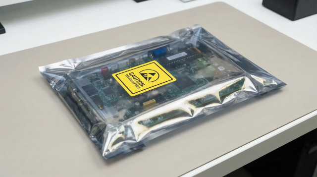
ESD performance is influenced not only by design but also by PCB manufacturing quality.
Important factors include:
Ground Connection Reliability
Reliable connections between:
- Components
- Ground planes
- Vias
are essential for effective ESD discharge.
PCB Material Selection
Material characteristics may affect:
- Insulation performance
- Moisture resistance
- Environmental reliability
Assembly Quality
Poor soldering or insufficient connection reliability may weaken ESD protection performance.
Manufacturing process control is important for maintaining long-term reliability.
8. Verification and Testing of ESD Performance
Before mass production, PCB designs should undergo ESD verification.
Common testing methods include:
- ESD immunity testing
- Contact discharge testing
- Air discharge testing
Testing helps evaluate whether the PCB can maintain:
- Functional stability
- Communication reliability
- Component protection
under real-world static discharge conditions.
Conclusion
ESD protection is an essential part of modern PCB design, especially as electronic systems become smaller, faster, and more integrated.
Effective anti-static design requires a combination of:
- Proper PCB layout
- Optimized grounding
- Suitable protection components
- Controlled signal routing
- Reliable manufacturing processes
By considering ESD protection during the early PCB design stage, engineers can reduce failure risks, improve product reliability, and create electronic systems capable of operating in more challenging environments.
