
Printed Circuit Board (PCB) manufacturing is a complex process that transforms a circuit design into a physical electronic platform capable of supporting components and enabling reliable electrical connections.
As the foundation of almost all electronic products, PCB quality directly influences:
- Electrical performance
- Product reliability
- Assembly efficiency
- Long-term operating stability
From consumer electronics and industrial control systems to automotive electronics, communication equipment, and medical devices, PCB manufacturing requires strict process control at every stage.
A complete PCB manufacturing process involves multiple steps, including:
- Engineering review
- Material preparation
- Inner layer fabrication
- Lamination
- Drilling
- Copper plating
- Outer layer imaging
- Surface finishing
- Inspection and testing
Each process step requires careful control to avoid defects such as:
- Open circuits
- Short circuits
- Layer misalignment
- Delamination
- Impedance variation
- Poor solderability
This article provides a detailed overview of PCB manufacturing processes and key precautions that engineers should consider before production.
1. Engineering Review and Manufacturing Preparation
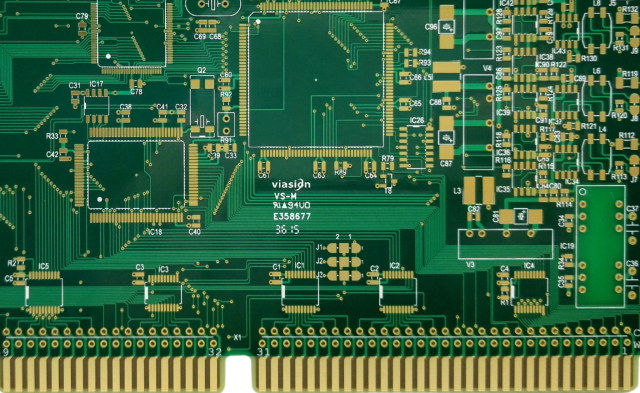
Before PCB fabrication begins, manufacturers perform an engineering review based on the customer’s design files.
Common input files include:
- Gerber files
- Drill files
- BOM files (for PCBA projects)
- PCB specifications
- Stack-up requirements
During this stage, engineers evaluate:
- Design manufacturability (DFM)
- Minimum trace width and spacing
- Via structures
- Material selection
- Layer configuration
- Manufacturing tolerances
Key Precautions
A comprehensive DFM review helps identify potential problems before production, such as:
- Insufficient copper spacing
- Improper via design
- Excessively small holes
- Difficult assembly structures
Early optimization can improve:
- Production yield
- Manufacturing efficiency
- Product reliability
2. Material Selection
PCB performance depends significantly on material selection.
Common PCB materials include:
FR-4 Materials
FR-4 is the most widely used PCB material.
Advantages:
- Cost-effective
- Good mechanical strength
- Mature manufacturing process
Applications:
- Consumer electronics
- Industrial control boards
- General electronic products
High-Tg FR-4 Materials
High-Tg materials provide improved thermal stability.
Advantages:
- Better heat resistance
- Reduced dimensional changes
Applications:
- Automotive electronics
- Industrial equipment
- High-reliability products
High-Frequency Materials
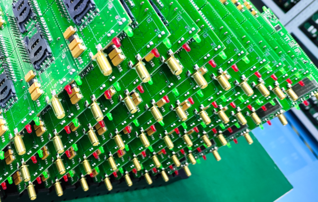
For RF and microwave applications, materials such as:
are selected.
Important parameters include:
- Dielectric constant (Dk)
- Dissipation factor (Df)
- Signal loss characteristics
3. Inner Layer Fabrication
For multilayer PCBs, inner layers are manufactured first.
The process includes:
3.1 Copper Laminate Preparation
Copper-clad laminates are cleaned and prepared.
Purpose:
- Remove contaminants
- Improve photoresist adhesion
3.2 Photoresist Coating
A photosensitive film is applied to the copper surface.
This layer defines the circuit pattern.
3.3 Exposure and Development
The circuit image is transferred using UV exposure.
The unwanted photoresist area is removed, exposing the copper that needs to be etched.
3.4 Etching
Chemical etching removes unnecessary copper.
The remaining copper forms the inner circuit pattern.
Key Precautions
Important controls include:
- Line width accuracy
- Copper thickness consistency
- Circuit pattern alignment
Poor control may cause:
- Signal integrity problems
- Electrical failures
- Layer connection issues
4. Automated Optical Inspection (AOI)
After inner layer fabrication, AOI equipment checks circuit patterns.
AOI detects:
- Missing traces
- Short circuits
- Copper defects
- Pattern deviations
This step prevents defective inner layers from continuing into later production stages.
5. Layer Alignment and Lamination
Multilayer PCBs require stacking multiple layers together.
The structure usually includes:
- Copper layers
- Prepreg
- Core materials
During lamination:
- Heat
- Pressure
- Time
are precisely controlled.
The resin melts and bonds all layers into one solid structure.
Key Precautions
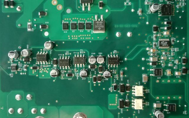
Lamination quality affects:
- Mechanical strength
- Electrical reliability
- Thermal performance
Common risks include:
- Delamination
- Resin voids
- Layer shifting
Proper stack-up design is essential for:
- Controlled impedance
- Signal integrity
- PCB reliability
6. CNC Drilling and Via Formation
Drilling creates holes for:
- Component mounting
- Electrical connections between layers
Types of vias include:
- Through vias
- Blind vias
- Buried vias
- Microvias
Key Precautions
Drilling parameters affect:
- Hole wall quality
- Plating reliability
- Signal performance
Important factors:
- Drill size
- Position accuracy
- Aspect ratio
Poor drilling can result in:
- Via cracks
- Open connections
- Reliability failures
7. Electroless Copper Plating
After drilling, hole walls are not conductive.
A copper plating process is used to create electrical connections.
The process includes:
- Hole cleaning
- Chemical activation
- Copper deposition
The copper layer connects:
- Different PCB layers
- Component pads
Key Precautions
Copper plating quality affects:
- Via reliability
- Current carrying capability
Potential issues include:
- Uneven copper thickness
- Poor hole coverage
- Via failure
8. Outer Layer Circuit Formation
The outer circuit pattern is created using similar imaging and etching processes.
The outer layer defines:
- Component pads
- Signal traces
- External connections
Precise control is required for:
- Fine-pitch components
- High-density PCB designs
9. Solder Mask Application
The solder mask protects exposed copper areas.
Functions include:
- Preventing oxidation
- Avoiding solder bridges
- Improving electrical insulation
Common colors include:
- Green
- Black
- Blue
- White
Key Precautions
Important considerations:
- Pad opening accuracy
- Solder mask thickness
- Surface cleanliness
Incorrect solder mask processing may cause:
- Poor soldering
- Assembly defects
10. Surface Finish Processing
Surface finish protects copper pads and improves solderability.
Common surface finishes include:
HASL (Hot Air Solder Leveling)
Advantages:
- Low cost
- Good solderability
ENIG (Electroless Nickel Immersion Gold)
Advantages:
- Flat surface
- Suitable for fine-pitch components
- Good corrosion resistance
Applications:
- HDI PCB
- High-density assemblies
ENEPIG
Advantages:
- Excellent reliability
- Suitable for advanced packaging
Applications:
- High-end electronic products
11. Electrical Testing
Electrical testing verifies PCB connectivity.
Common methods include:
Flying Probe Testing
Suitable for:
- Prototype production
- Low-volume orders
Fixture Testing
Suitable for:
- Mass production
Tests include:
- Open circuits
- Short circuits
- Resistance values
12. Final Inspection and Packaging
Before shipment, PCB manufacturers perform final inspections.
Inspection items include:
- Appearance inspection
- Dimension measurement
- Surface quality
- Packaging protection
Proper packaging prevents:
- Moisture absorption
- Mechanical damage
- Surface contamination
13. Important Precautions During PCB Manufacturing
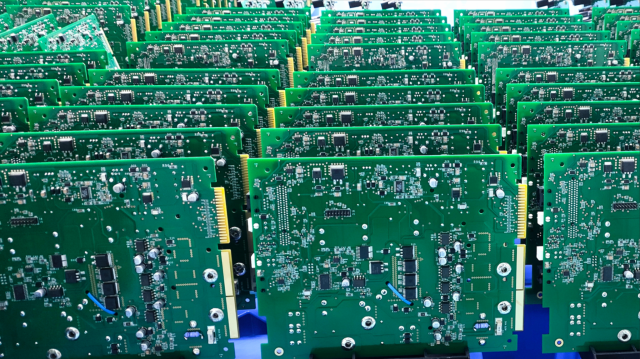
13.1 Maintain Accurate Stack-Up Design
A correct stack-up ensures:
- Stable impedance
- Better signal transmission
- Reduced EMI issues
13.2 Control Impedance Requirements
For high-speed designs, impedance control is critical.
Factors include:
- Trace width
- Copper thickness
- Dielectric thickness
- Material properties
Common requirements:
- 50Ω single-ended impedance
- 90Ω/100Ω differential impedance
13.3 Consider Thermal Management
High-power PCB designs require attention to:
- Copper thickness
- Thermal vias
- Heat dissipation paths
13.4 Follow DFM Principles
Design should consider manufacturing capability:
- Minimum spacing
- Drill limitations
- Assembly requirements
- Testing accessibility
13.5 Select Appropriate Surface Finish
The surface finish should match:
- Component type
- Assembly process
- Reliability requirements
Conclusion
PCB manufacturing is a highly coordinated process involving material selection, circuit fabrication, lamination, drilling, plating, surface treatment, inspection, and testing.
Every manufacturing stage can influence final PCB performance. Therefore, successful PCB production requires:
- Accurate engineering review
- Proper material selection
- Strict process control
- Reliable inspection methods
- Effective DFM optimization
By understanding PCB manufacturing processes and precautions, engineers can improve product reliability, reduce production risks, and achieve smoother transition from prototype development to mass production.
