How to Check for PCB Warpage: Techniques and Methods
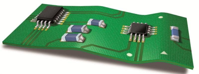
PCB warpage (also known as bow and twist) is a common manufacturing defect that occurs when a printed circuit board deviates from perfect flatness. It can lead to serious issues during SMT assembly, such as poor solder joint formation, component misalignment, open circuits, or bridging. In industrial applications, excessive warpage may cause reliability problems in automation equipment, control systems, and harsh-environment electronics.
At KKPCB, we implement strict warpage control throughout the production process and offer comprehensive inspection services to ensure every board meets high-reliability standards for industrial use.
Understanding PCB Warpage: Bow vs. Twist
- Bow: The board curves in a cylindrical or spherical shape, with all four corners remaining in approximately the same plane while the center lifts or dips.
- Twist: The board deforms diagonally, causing one corner to lift while the other three remain in contact with a flat surface.
Both types are measured as a percentage of the board’s diagonal length. Early detection helps prevent downstream assembly failures and costly rework.
IPC Standards for Acceptable Warpage
According to IPC-6012 and related specifications:
- For boards using surface-mount components (SMT): Maximum bow and twist ≤ 0.75%.
- For through-hole only boards: Maximum ≤ 1.5%.
- High-reliability applications (Class 3, e.g., industrial control, medical, aerospace): Often tightened to ≤ 0.5% or even 0.3% by customer specification.
Calculation Example: For a PCB with a 400 mm diagonal, the maximum allowable warpage height at 0.75% is approximately 3 mm. Warpage % = (Maximum deviation height / Diagonal length) × 100
IPC-TM-650 Method 2.4.22 defines the standard test procedure for bow and twist measurement.
Common Techniques and Methods to Check PCB Warpage
Here are proven methods ranging from simple manual checks to advanced automated systems:
- Visual Inspection & Granite Surface Plate Method (Basic) Place the PCB on a calibrated flat granite or glass surface plate. Observe if all corners lie flat or if gaps appear. This is a quick preliminary screening but lacks precision.
- Feeler Gauge (Pin Gauge) Method (Common & Cost-Effective)
- Calculate the maximum allowable gauge thickness based on board dimensions and IPC limit (e.g., RL = Length × 0.75 / 100).
- Insert feeler gauges under the highest point while three corners touch the surface.
- Suitable for routine quality checks and go/no-go decisions. Good for detecting significant warpage.
- Height Gauge or Dial Indicator Use a precision height gauge or dial indicator on a surface plate to measure the exact height difference between the highest and lowest points. Provides accurate readings in millimeters with 0.01 mm resolution.
- Three-Point or Four-Point Measurement Restrain three corners on a flat surface and measure the lift at the fourth corner. This is particularly effective for assessing twist.
- Laser Scanning & 3D Optical Profilometry (High Precision) Non-contact laser or optical systems scan the entire board surface to generate a 3D topography map. Ideal for complex shapes, large panels, and high-volume production. Offers sub-millimeter accuracy and fast data capture.
- Shadow Moiré and Fringe Projection Methods These optical interferometry techniques are recommended in IPC-9641 for high-temperature warpage measurement (simulating reflow conditions). They provide detailed local area warpage data across thermal profiles.
- Automated Optical Inspection (AOI) and Coordinate Measuring Machines (CMM) Integrated into production lines for real-time detection. Advanced systems combine vision with laser for full-surface mapping.
- Reflow Simulation Warpage Testing Measure warpage before, during, and after a simulated reflow profile to predict behavior in actual SMT assembly.
Pro Tip: Always perform measurements in a controlled environment (temperature and humidity) and consider baking boards (e.g., 10°C above Tg for 20 minutes followed by controlled cooling) to distinguish between reversible (moisture-induced) and permanent warpage.
Why Warpage Matters in Industrial PCB Production
In industrial environments, boards often face vibration, wide temperature swings, and mechanical stress. Even minor warpage can lead to:
- Component placement errors
- Solder joint stress and early failure
- Reduced yield in high-density HDI or multilayer designs
- Issues with heavy copper or rigid-flex structures
KKPCB uses advanced multilayer lamination, symmetric stack-up design, balanced copper distribution, and rigorous DFM analysis to minimize warpage from the design stage onward.
Best Practices to Prevent and Control Warpage
- Optimize copper balance across layers
- Use symmetric stack-ups and compatible (matched CTE)
- Select high-Tg or low-CTE laminates for demanding applications
- Implement proper lamination pressure, temperature, and cooling profiles
- Conduct incoming material inspection and post-production warpage checks
- Provide DFM feedback early in the project
At KKPCB, our quality team performs warpage inspection on every batch using a combination of IPC-compliant methods and precision equipment, ensuring boards are production-ready for industrial automation, new energy systems, and control equipment.
Need help verifying warpage on your industrial PCB design or prototype? Send us your Gerber files or specifications. Our engineers will provide detailed DFM analysis, warpage risk assessment, and optimized manufacturing solutions.
