
Designers often discover aspect-ratio limits late, when a fabricator asks to enlarge vias on a thick backplane or test board. This guide explains how aspect ratio is calculated, why it matters for plating reliability, which limits apply to through-holes and microvias, and how to design within KKPCB’s published manufacturing capabilities.
1. How to Calculate PCB Aspect Ratio
For a plated through-hole:
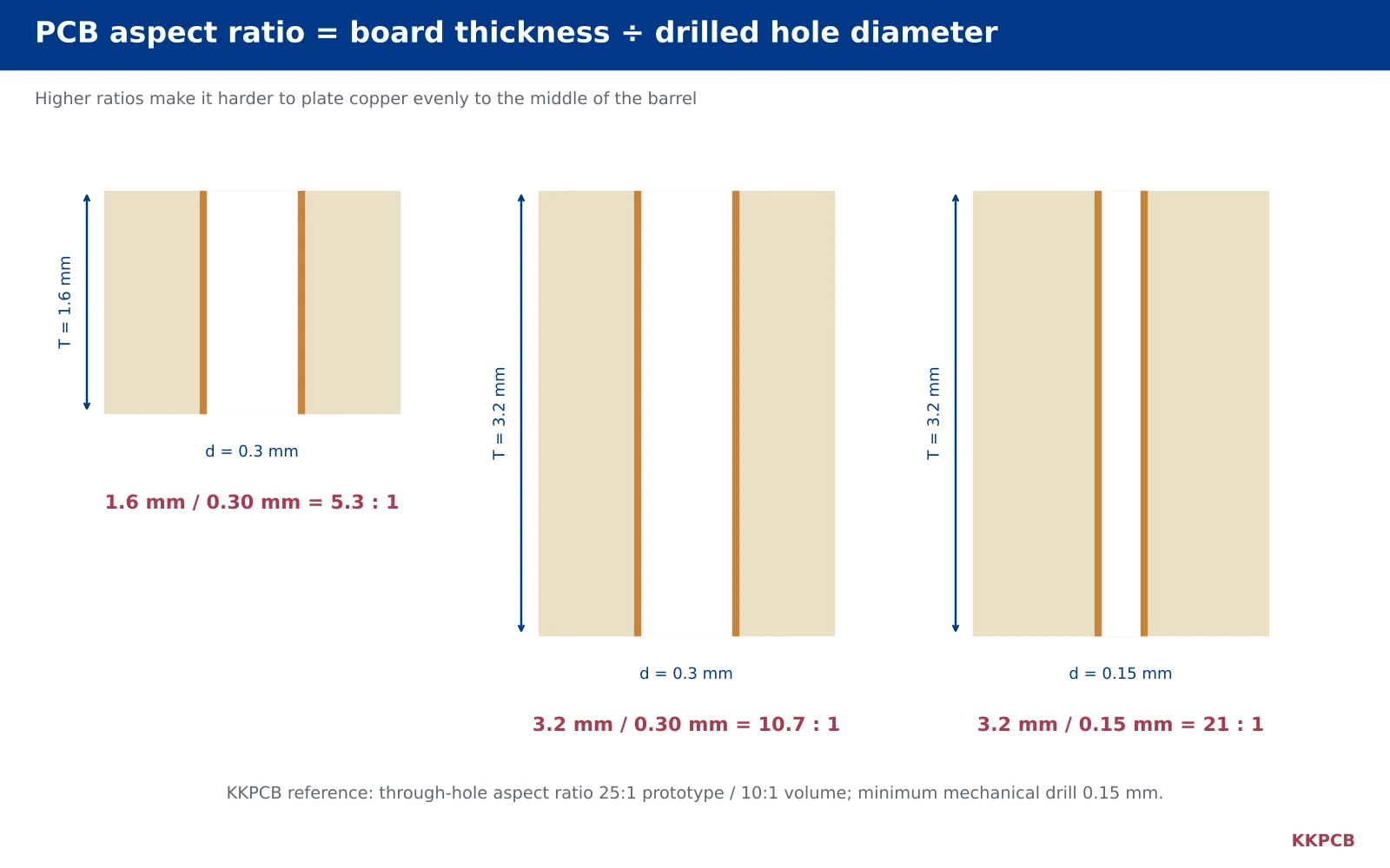
Aspect ratio = board thickness ÷ drilled hole diameter
Examples:
- 1.6 mm board, 0.30 mm drill: 1.6 ÷ 0.30 = 5.3:1
- 3.2 mm board, 0.30 mm drill: 3.2 ÷ 0.30 = 10.7:1
- 3.2 mm board, 0.15 mm drill: 3.2 ÷ 0.15 = 21:1
Fabricators normally calculate with the drilled diameter, which is larger than the finished hole size shown in many design tools because plating reduces the diameter. Always check which value your CAD output and fabrication notes refer to.
For blind microvias the ratio is calculated from the via depth (the dielectric thickness being drilled) and the laser hole diameter.
2. Why PCB Aspect Ratio Matters
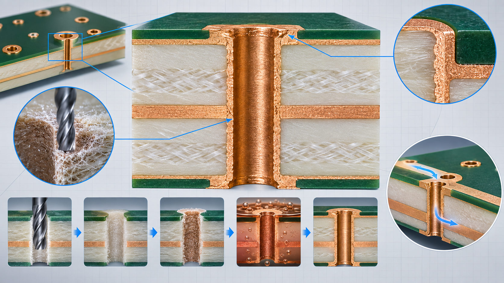
Copper is deposited in a via barrel by electroplating. The plating solution has to flow into the hole and current has to reach its centre. In a short, wide hole this is easy; in a long, narrow hole the centre of the barrel receives less copper than the ends. Engineers call the ability to plate evenly “throwing power”.
When the aspect ratio is too high for the process, typical problems include:
- Thin copper in the middle of the barrel, below the specified minimum.
- Barrel cracks during thermal cycling or reflow, because thin copper cannot absorb the z-axis expansion of the laminate.
- Voids where plating solution did not wet the hole wall properly.
- Drill deflection in small, deep holes, causing registration errors on inner layers.
IPC-6012 sets minimum average copper thickness in plated holes – 20 µm for Class 2 and 25 µm for Class 3 – and those values must be achieved in the middle of the barrel, not just at the surface. Higher aspect ratios make that harder.
3. PCB Aspect Ratio Limits at KKPCB
| Feature | KKPCB reference |
|---|---|
| Through-hole aspect ratio | 25:1 prototype; 10:1 small and medium volume |
| Mechanical drill diameter | 0.15–6.50 mm |
| PTFE / mixed-material minimum drill | 0.25 mm |
| Finished board thickness | 0.10–8.00 mm prototype; 0.25–6.50 mm volume |
| Laser microvia | 0.10 mm hole for depth ≤55 µm; 0.13 mm for depth ≤100 µm |
| ATE test boards (special process) | Up to 50:1 drilling and plating references; 42:1 via filling |
The difference between the prototype and volume columns is intentional. A 25:1 hole can be built and verified on a prototype run, but 10:1 is the value to design around if the board must move into stable production without changes. ATE probe-card and load boards are a special category with dedicated drilling and plating processes; see ATE PCB & probe card.
4. Minimum Drill Size by Board Thickness
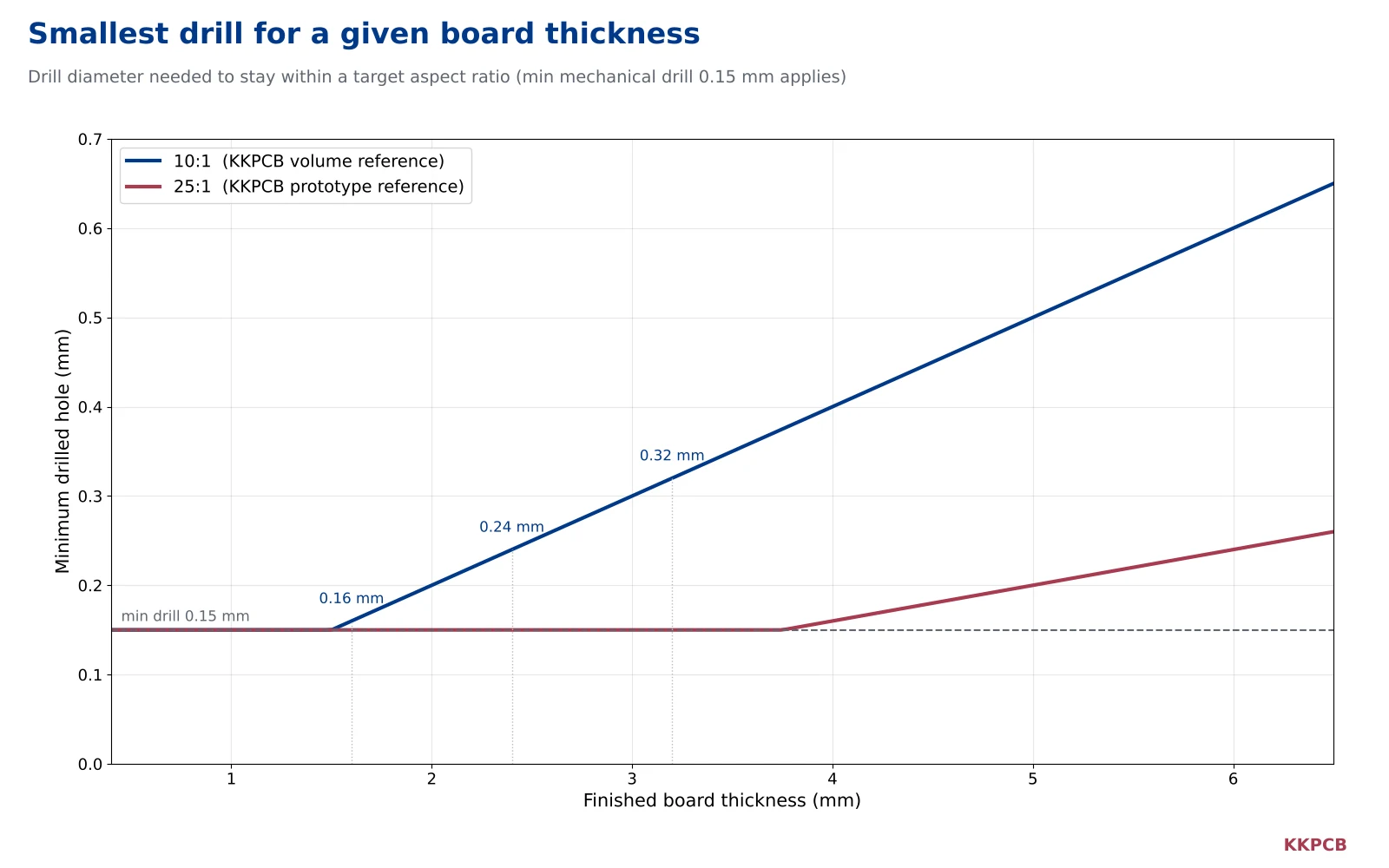
Combining the aspect-ratio limit with the 0.15 mm minimum mechanical drill gives a quick way to choose via sizes:
| Board thickness | Smallest drill at 10:1 (volume) | Smallest drill at 25:1 (prototype) |
|---|---|---|
| 1.0 mm | 0.15 mm (minimum drill applies) | 0.15 mm (minimum drill applies) |
| 1.6 mm | 0.16 mm | 0.15 mm (minimum drill applies) |
| 2.4 mm | 0.24 mm | 0.15 mm (minimum drill applies) |
| 3.2 mm | 0.32 mm | 0.15 mm (minimum drill applies) |
| 4.0 mm | 0.40 mm | 0.16 mm |
| 6.0 mm | 0.60 mm | 0.24 mm |
These are geometric limits only. Material, copper weight, layer count and hole density also affect what is practical, so treat the table as a starting point for DFM review rather than a guarantee.
5. Microvia Aspect Ratio
Laser microvias are shallow and have their own rules. Because the hole is blind, plating solution cannot flow through it, so microvias are normally kept at or below roughly 1:1 depth-to-diameter. KKPCB’s HDI references show what that means in practice: a 0.10 mm laser hole for a dielectric up to 55 µm deep, and 0.13 mm for up to 100 µm.
Stacked microvias add a second requirement: each via must be completely copper-filled so that the next via can land on it. Read more in our guides to any-layer HDI PCB and via in pad.
6. How to Design Within PCB Aspect Ratio Limits
Size vias by board thickness, not habit
A 0.20 mm via is easy on a 1.6 mm board (8:1) but becomes 16:1 on a 3.2 mm board. Re-check via sizes whenever the stack-up thickness changes.
Use blind and buried vias to shorten holes
If a signal only needs to travel between a few layers, a blind or buried via keeps the drilled depth – and the aspect ratio – small. This is common on thick high-layer-count boards.
Consider backdrilling for high-speed stubs
Backdrilling removes the unused part of a through-hole barrel to reduce stub length. It does not change the original plating requirement, so the through-hole must still be plateable. KKPCB’s backdrill references include a minimum backdrill diameter of 0.20 mm for PTH and a depth tolerance of ±0.15 mm (prototype).
Separate large and small holes
Very different hole sizes on the same board compete for plating current. Discuss with your fabricator whether hole sizes can be grouped or whether a different plating approach is needed.
Specify the class and copper thickness
State IPC class and minimum barrel copper on the fabrication drawing so the fabricator can plan the plating process accordingly.
7. PCB Aspect Ratio in High-Layer-Count and Thick Boards
High-layer-count backplanes, test boards and power boards are where aspect ratio becomes critical. A 30-layer board can easily exceed 3 mm in thickness, which pushes standard vias beyond 10:1 unless the drill size is increased. Heavy copper on inner layers increases thickness further. KKPCB supports 1–40 layers (above 30 by review); for these builds, aspect ratio, copper weight and material should be reviewed together at the stack-up stage. Our multilayer PCB page lists typical constructions.
8. Worked Example: A 24-Layer, 3.2 mm Board
Consider a 24-layer networking board, 3.2 mm thick, with a BGA that the designer would like to fan out with 0.20 mm vias.
- Calculate the ratio: 3.2 ÷ 0.20 = 16:1. That is above the 10:1 volume reference, so the design would only be suitable for prototypes unless something changes.
- Option A – enlarge the drill: a 0.32 mm drill gives 10:1, which suits volume production but needs larger pads and may not fit the BGA pitch.
- Option B – shorten the via: if most BGA signals only need to reach the first few inner layers, blind vias or a sequential-lamination structure keep the drilled depth small and the ratio low.
- Option C – reduce thickness: thinner dielectrics or fewer plane layers reduce board thickness, but impedance and power-delivery requirements must still be met.
- Decision: in practice the best answer is often a combination, such as through-holes of 0.30 mm for power and long nets, with blind vias for the dense BGA breakout.
This kind of trade-off is easiest when it is discussed before routing starts, because changing drill sizes after layout usually means moving pads and traces.
9. How Fabricators Control Plating in High-Aspect-Ratio Holes
When a design does require deep, narrow holes, several process controls make reliable plating possible:
- Drill quality: sharp, correctly specified drill bits, appropriate feed rates and limited hits per bit keep hole walls smooth and positions accurate.
- Hole wall preparation: desmear and metallization must reach the full depth of the hole so that plating can start uniformly.
- Plating chemistry and current control: solutions and current waveforms designed for high throwing power deposit more copper in the centre of the barrel relative to the surface.
- Solution movement: agitation and flow through the holes renew the electrolyte inside the barrel.
- Verification: microsections measure copper thickness at the centre of the barrel, where it is thinnest, and thermal stress tests confirm that the barrel survives reflow temperatures.
These controls are also why prototype and volume limits differ: a prototype run can be tuned and fully inspected, while volume production needs a process window that is stable lot after lot.
10. PCB Aspect Ratio Checklist for Your RFQ
| Item to provide | Reason |
|---|---|
| Finished board thickness and tolerance | Defines the length of every through-hole |
| Drill table with drilled and finished sizes | Removes ambiguity in the aspect-ratio calculation |
| Drill spans for blind, buried and through vias | Each span has its own depth and ratio |
| IPC class and minimum barrel copper | Sets the plating target that must be reached in the hole centre |
| Backdrill locations and target stub length | Backdrill depth and diameter must be planned with the stack-up |
| Material type, especially PTFE or hybrid | Minimum drill and hole preparation differ by material |
| Expected volume | Determines whether prototype or volume limits apply |
Frequently Asked Questions
What is a good PCB aspect ratio?
For standard production, keep through-holes at or below 10:1. Higher ratios are possible – KKPCB supports up to 25:1 for prototypes – but they should be confirmed with the fabricator before layout is finalized.
Is PCB aspect ratio calculated with finished or drilled hole size?
Fabricators usually use the drilled hole diameter. Because plating reduces the hole, the finished diameter is smaller, so a calculation with the finished size will overstate the aspect ratio.
What happens if my design exceeds the aspect-ratio limit?
The fabricator will usually ask to enlarge the drill, reduce board thickness, or convert the via to a blind or buried structure. Exceeding the limit without changes risks thin barrel copper and reliability failures.
Does aspect ratio apply to microvias?
Yes, but with a different limit. Laser microvias are blind holes, so they are normally kept at about 1:1 depth-to-diameter or lower.
Why do ATE boards allow much higher aspect ratios?
ATE load boards and probe-card boards are very thick and use dedicated drilling, plating and filling processes. KKPCB lists 50:1 drilling and plating references for this category, which are not standard values for general PCBs.
Get a PCB Aspect Ratio Check from KKPCB
KKPCB reviews drill size, board thickness and plating requirements together during DFM, from PCB prototype to volume PCB manufacturing.
Working on a thick or high-layer-count board? Contact KKPCB with your stack-up and drill data for an aspect-ratio review.
PCB fabrication at KKPCB follows the acceptance criteria of IPC (IPC-6012, IPC-A-600).