
A Satellite PCB Ku-band feed network is often released as a routing problem, then fails as an integration problem. The electrical design may show equal-length branches and an acceptable nominal impedance, yet the assembled payload can lose phase balance when a connector launch, via fence, housing wall, or harness datum moves the return path. At Ku-band, millimetres of unintended geometry and a small change in dielectric thickness can consume the margin reserved for the antenna or transceiver. This guide describes a practical release method for engineers and project managers who need a controlled feed network rather than a visually symmetric drawing.
Define the feed-network intent before drawing copper
For a Satellite PCB Ku-band feed network, the first review should state what the network must preserve: branch-to-branch phase balance, insertion-loss budget, return loss, polarization relationship, power level, and the environmental range. A Satellite PCB Ku-band feed network using a high-frequency PCB cannot be judged only by its room-temperature appearance. The network might distribute a local oscillator, connect a phased-array element, or route a transceiver path through a constrained satellite panel. Each use has a different tolerance for amplitude error, phase error, and connector repeatability.
Write the electrical intent next to the mechanical datum. Identify the RF input, output ports, antenna or module boundary, chassis wall, fasteners, and shield edge. A Satellite PCB Ku-band feed network PCB layout review should then show which reference plane carries the return current and which objects are allowed to interrupt it. This prevents the common late-stage change in which a mounting hole is added through a ground fence or a harness keep-out forces one branch around a different layer.
For a project manager, the useful deliverable is a one-page interface definition: port names, connector family, board datum, target frequency band, allowable branch mismatch, and the evidence required at release. Without this page, each supplier may interpret “matched feed” differently and the first integrated build becomes the only place where the disagreement is discovered.
Lock material and stack-up variables
A Satellite PCB Ku-band feed network depends on finished geometry, not just a laminate trade name. Record the dielectric family, finished dielectric thickness, copper weight, glass style, resin content, solder mask, and press construction. The PCB materials decision should identify which values are typical design inputs and which are acceptance limits. If the design uses a low-loss RF core beside a digital core, mark the transition and the vias that cross it.
Use a controlled PCB manufacturing stack-up that the fabricator can hold after pressing, plating, and etching. A nominal trace width calculated from an ideal dielectric thickness is not sufficient. Include etch compensation, copper roughness assumptions, solder-mask clearance, and the finished tolerance used by the impedance coupon. The drawing should define the reference-plane separation that makes the Satellite PCB Ku-band feed network phase model meaningful.
Thermal and mechanical assumptions also belong in this review. A dense copper region under a power device can change the local press balance, while a chassis fastener can constrain expansion at one end of the board. If a multilayer PCB uses hybrid materials, release the layer-to-layer material map, the via construction, and the drill registration window together. This makes a later material substitution visible before it changes electrical length.
Build equal electrical paths, not merely equal-looking paths
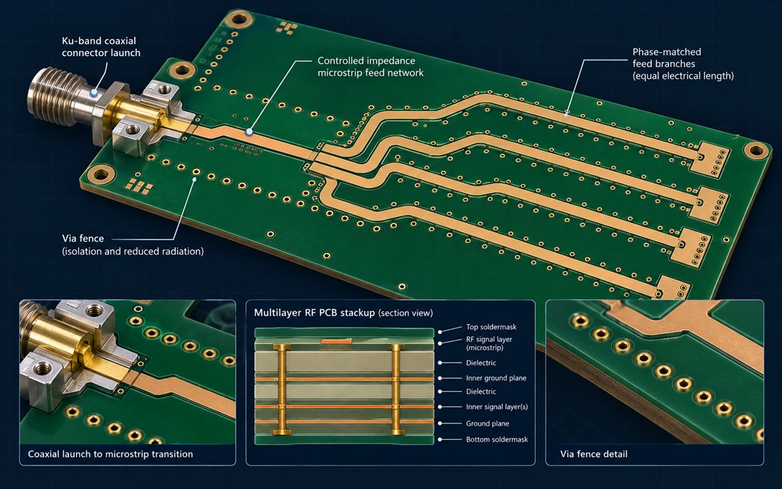
For a Satellite PCB Ku-band feed network, equal physical length is only a starting point. A branch that changes layer through a via, passes a connector cut-out, or uses a different bend radius can have a different effective phase delay. Keep branch topology consistent: the same number of layer transitions, comparable bend geometry, matched reference-plane environment, and similar via-fence spacing. A controlled-impedance PCB check should calculate the launch, trace, bend, and termination as one channel.
Reserve a continuous return corridor beside every branch. Ground vias should be close enough to contain the field but not so close that drill registration, solder mask, or etch compensation becomes the dominant risk. Where the network approaches an antenna or filter, keep the reference plane continuous and document any intentional slot. If the board includes a RF PCB transition, review the electric field boundary and the mechanical clearance in the same view.
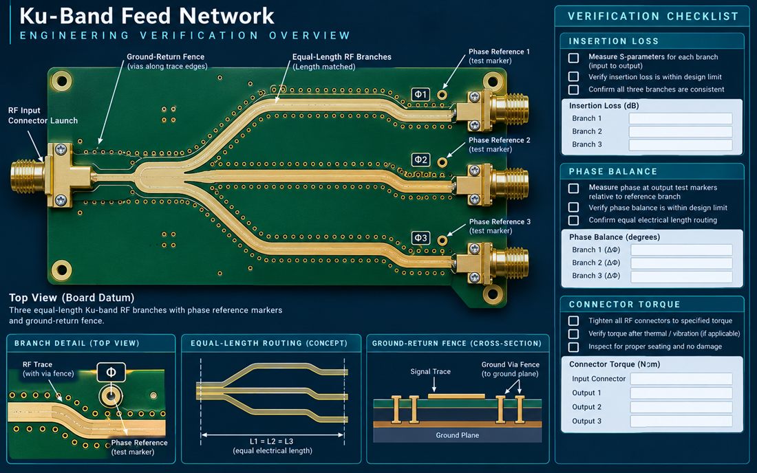
Use the branch centerline, not the outer edge of the copper, as the comparison datum. Capture the effective length, number of bends, via count, and distance to the nearest ground feature. This lets the designer explain a Satellite PCB Ku-band feed network phase difference as a controlled geometry delta rather than an unexplained result from a black-box simulator. It also gives manufacturing a short list of dimensions to inspect on the panel.
Treat connector launch and via fence as one interface
In a Satellite PCB Ku-band feed network, a coax launch can be electrically correct on a bare coupon and still fail when the connector body is tightened against a spacecraft bracket. Define pad diameter, anti-pad, ground tabs, mounting holes, connector seating, and the first return vias from one mechanical datum. A PCB prototype should reproduce the same launch stack and edge constraints as the flight-like board; otherwise the prototype validates a different interface.
For high-density launches, inspect the drill-to-copper clearance and the barrel position relative to the signal pad. The rigid-flex PCB option may reduce harness stress, but the stiffener, bend zone, and shield termination must not interrupt the RF return. If a board-edge connector is used, add a connector keep-out and a torque or insertion-force note to the same release package.
Panelization is another hidden variable. Keep the RF edge away from breakaway tabs, tooling holes, and coupons that may disturb copper balance. A DfMA review should confirm routing of the panel, depanelization method, plating support, and inspection access before the feed network is frozen.
Release a verification vehicle with useful evidence
For a Satellite PCB Ku-band feed network, do not make the first Satellite PCB Ku-band feed network production panel the only test vehicle. Define a coupon or release vehicle with the same dielectric thickness, copper, launch, return fence, and connector mounting. The measurement plan can record S-parameters, branch-to-branch phase balance, connector repeatability, and visual evidence of the launch. Results should be labeled as design-verification data for that vehicle, with frequency, temperature, calibration, fixture, and connector torque documented.
The Satellite PCB Ku-band feed network assembly traveler should identify the solder profile, cleaning method, bake condition, shield installation, and inspection points. PCB assembly changes can alter the launch through solder fillet shape or connector seating. Use quality control records to tie the measured board to the artwork revision, stack-up, copper lot, and panel serial.
When a component or connector becomes unavailable, component sourcing must compare package geometry, pin field, mounting datum, plating, and RF transition—not only the part number. A substitution that fits the schematic can still change phase balance or the return path. For the project gate, list open assumptions and decide whether a new coupon, a new launch fixture, or a repeat assembly build is required.
Handoff and change control for the program team
Before release, the design owner should deliver a single controlled package containing the stack-up, impedance targets, port definition, branch geometry, launch drawing, panel drawing, coupon plan, assembly notes, and change log. The PCB assembly capabilities review should verify that the connector, shield, and test points can be built and inspected without adding an uncontrolled rework step.
Use aerospace PCB assembly controls when environmental evidence matters, and use PCB capabilities for the live manufacturing scope. Finally, keep standard PCB capacity and the high-frequency process window visible in the quote and build plan so that a schedule decision does not silently change the RF construction.
A Satellite PCB Ku-band feed network is ready when its electrical intent, material assumptions, launch mechanics, manufacturing limits, and verification evidence describe the same physical object. That alignment reduces late surprises and gives the program team a defensible basis for approving a change or repeating a build.
Sources: laminate manufacturer RF and dimensional-stability data; NASA workmanship guidance; Analog Devices high-frequency layout notes; Qorvo packaging and RF-transition guidance; Würth RF PCB references; and connector manufacturer application data. Values are engineering targets or typical design inputs, not customer measurements.





