
Satellite PCB radiation design for low-Earth-orbit avionics is often reviewed too late as a materials choice. The difficult question is not whether a board can route a signal; it is whether the dielectric, copper stack, enclosure bond, and return current still behave predictably after radiation exposure, thermal cycling, launch handling, and repeated engineering changes. A project team needs a release method that connects component risk to the physical board before a prototype is frozen.
Why Satellite PCB radiation design changes a board-level decision
In a spacecraft electronics module, total-ionizing-dose exposure, single-event effects, and charging mechanisms can change how a mixed-signal channel is interpreted. The PCB is not a radiation shield by itself. Its plane geometry determines where transient currents return, how shield seams are bonded, and how much sensitive copper is exposed to an enclosure boundary. A receiver, ADC, memory device, or clock buffer may have a different upset sensitivity, so placing every interface on one common copper corridor makes later mitigation expensive.
Begin the review with a zone map: noisy converters and switching nodes, RF launches, precision analog, timing, and service connectors. Record the intended current corridor for every zone, then verify that the stack-up gives each corridor a continuous reference plane.
Choose the dielectric and copper stack as a coupled system
Engineers often select a laminate from a nominal dielectric constant and then ask manufacturing to make the geometry fit. That sequence is risky for a satellite payload because effective permittivity depends on resin content, glass style, frequency, copper roughness, and the finished press cycle. A practical Satellite PCB release therefore fixes the impedance target, finished dielectric thickness, copper weight, and etch compensation together.
For a controlled RF path, define the target as a design value with tolerance rather than a single laboratory number. If a 50-ohm microstrip is sensitive to enclosure height, put the enclosure datum and solder-mask assumption on the drawing instead of leaving them in an engineer’s notebook.
A multilayer spacecraft board also needs a mechanical interpretation. Heavy copper around a connector or chassis bond can create local resin starvation, uneven press flow, and a thermal gradient that moves the launch. Use balanced copper distribution, keep drilled transitions away from abrupt plane voids, and review the annular-ring margin at the same time as the impedance coupon.
A Satellite PCB intended for a Ku- or Ka-band front end should not rely on a generic coupon that is disconnected from the actual launch stack. The coupon should preserve the same reference-plane spacing and copper family as the flight panel.
Build a return-path boundary around mixed-signal zones
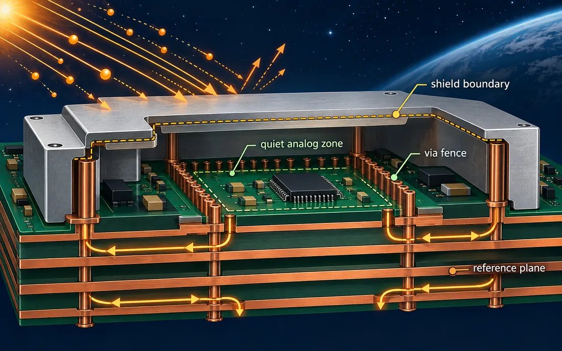
Radiation reviews are frequently separated from signal-integrity reviews, even though both depend on return-path continuity. A split plane that looks harmless at DC can force an RF or clock return to detour around a keep-out. That detour increases loop area and makes the board more sensitive to enclosure seams, cable shields, and connector mounting torque.
Use stitching vias at the boundary of a shielded RF island, but do not place them so close to a high-speed trace that their anti-pads erase the reference plane. A useful rule is to define the return-path boundary in the stack-up drawing and in the placement constraint file, not only on a redline image.
For the layout owner, the Satellite PCB checklist should include: uninterrupted reference metal under each critical transition; a via fence tied to the intended chassis or signal ground; short paths from connector grounds to the fence; and a documented bridge where analog and digital returns meet. The bridge is a controlled connection, not an invitation to pour copper everywhere.
If an RF module must cross from a shield can to a board-edge connector, reserve the return vias before routing the signal pair. This prevents a late mechanical change from consuming the only low-inductance path.
Keep RF, ADC, and clock domains from sharing the wrong current corridor
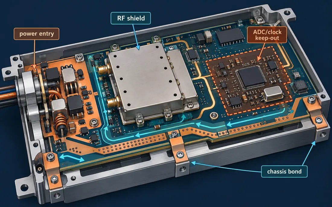
A small satellite payload may combine a low-noise receiver, an ADC, a high-speed serial link, and a power converter on a board that is only a few centimeters wide. The common project failure is not an obviously bad trace; it is a shared corridor that allows converter ripple, clock harmonics, and RF return current to pass through the same neck.
Treat each zone as a current budget.
Define where the power return enters, where the chassis bond is made, and which plane carries the transient current. A Satellite PCB material review should then ask whether the chosen dielectric, copper roughness, and loss tangent support the required link margin at the highest operating frequency.
The component placement review should include the clock source, ADC reference, LDOs, ferrites, and connector shields. Keep the ADC reference loop compact and give its return a quiet route that does not cross a switching-node void. For an RF front end, keep the launch and first filter section in the same geometric environment as the verification coupon.
For this Satellite PCB, the return-path record should accompany the test plan.
The resulting design is easier to debug because a phase or noise change can be traced to a stated plane, via, or connector datum rather than to an unexplained “RF layout issue.”
Assembly and DFM controls before environmental qualification
Each Satellite PCB project can lose schedule when assembly is treated as a separate activity. Space-oriented boards need the assembly constraints recorded before the layout is frozen. A documented high-frequency PCB capabilities review should check solder-mask registration, exposed copper near RF launches, connector coplanarity, and rework access before ordering panels.
A multilayer PCB stack should also be checked for press symmetry and drill-to-copper clearance.
When a board is assembled, a PCB assembly traveler should identify cleaning chemistry, bake conditions, moisture controls, and inspection points around shield cans and fine-pitch packages.
Before a Satellite PCB reaches environmental qualification, the project manager should require a DfMA review tied to the exact revision. Confirm that component sourcing substitutions cannot move a clock, ADC, or RF filter into a different return zone. Use quality control records to link coupons, panel IDs, drill data, and inspection images to the release package.
If the payload uses a flexible interconnect, a rigid-flex PCB review must include bend radius, shield continuity, and connector strain relief rather than treating the flex as a cable.
A release checklist for the project team
- Freeze the radiation, thermal, frequency, and mechanical assumptions that influence the stack-up.
- Map every RF, ADC, clock, power, and chassis return path on the same revision as the layout.
- Correlate the coupon geometry with the actual launch, reference spacing, copper family, and solder-mask state.
- Verify that shield fences and connector grounds remain manufacturable after panelization and assembly.
- Record substitutions, rework limits, cleaning steps, and inspection evidence in the release package.
- Ask the aerospace PCB assembly team to sign the interface checklist before qualification.
For a Satellite PCB release, the project owner should sign the radiation zone map, the Satellite PCB stack-up assumptions, and the Satellite PCB assembly traveler as one package. This keeps the Satellite PCB design intent visible when a revision moves from prototype to qualification.
These controls make a PCB prototype useful as an engineering decision, not merely as a board that powers on. They also leave a defensible path from material selection to flight-like verification without claiming a customer measurement that has not been recorded. Sources: laminate manufacturer technical data and application notes; NASA workmanship and contamination-control guidance; Analog Devices and Qorvo mixed-signal and RF layout notes; and Würth signal-integrity reference material.
Values described here are design ranges or engineering targets, not customer test results.





