
A pulse oximeter combines timed LED drive with a sensitive optical receive path. Red and infrared LEDs are pulsed, while a photodiode and analog front end measure a much smaller returned signal. On a Healthcare PCB, the design challenge is to keep the high-current drive edges and their supply return from disturbing the photodiode input, while preserving the optical geometry and timing required by the selected system. A board layout alone cannot establish clinical accuracy or device compliance. A Healthcare PCB review should treat the optical, electrical, mechanical, and firmware interfaces as one configuration.
Map the Healthcare PCB optical signal chain
For a Healthcare PCB, draw the path from the LED driver through the red and infrared emitters, sensor window, optical path, photodiode, transimpedance amplifier, filter, converter, processor, and data interface. Mark LED supply rails, switching converters, reference voltages, timing lines, and every ground return. That map lets the layout separate pulsed transmit current from high-impedance receive nodes without losing the actual return path. TI’s AFE4404 is one optical biosensing example; its device information describes three switching LEDs and one photodiode. That device-specific arrangement is not a prescription for every oximeter. Follow the selected AFE data sheet and timing diagram. A multilayer PCB stackup should show the transmit and receive routes layer by layer.
Define the analog reference from the circuit rather than drawing an arbitrary “quiet ground” island. A split under an amplifier may interrupt its return; a shared narrow plane neck may let LED or converter current move the reference. Mark where each current enters and closes, then show intentional tie points, shield connections, sensor connectors, and chassis contacts. Keep LED supply returns away from the photodiode feedback network where the chosen circuit allows it. A PCB design review should pair the schematic return map with the routed stackup.
Keep LED pulse current local
On a Healthcare PCB, place the LED driver, local bypass capacitors, and current-setting components near the AFE or sensor connector as specified by the selected device documentation. Keep the current loop compact from supply through driver and emitter and back to its return. Avoid sharing a narrow trace or via neck with the receiver reference, photodiode return, or converter feedback. The LED current and pulse sequence depend on the selected optical design; do not copy a generic current value from a different reference design. A Healthcare PCB prototype can help compare supply transients and receiver behavior on a documented revision.
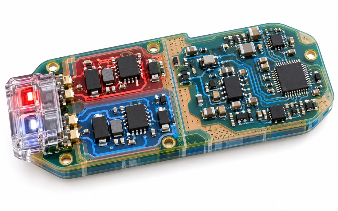
Keep fast drive edges and converter switch nodes away from the photodiode input, transimpedance feedback parts, and ADC reference. Route the outgoing and return conductors together, minimize unnecessary switch-node copper, and place decoupling at the driver pins. If the optical sensor is remote, include the cable and its return in the current-loop review. A shield or large copper shape can change current paths, optical clearance, and heat flow, so define its role before adding it. A PCB fabrication review should preserve sensor openings and keepouts through panelization and edge tolerances.
Protect the photodiode and transimpedance path
The Healthcare PCB photodiode signal can be sensitive to parasitic capacitance, leakage, contamination, and coupled edges. Keep the input trace short, avoid unnecessary vias, and place feedback components close to the amplifier pins according to the selected circuit. Keep clocks, LED switching, and converter nodes away from the input and feedback network. Check input protection for capacitance and leakage appropriate to the design. Do not route a fast edge beneath the receiver region unless the AFE guidance and measured results support that arrangement.
Track the receiver reference through the amplifier, ADC, decoupling, and sensor connector. A low-impedance point can still move if a pulsed return shares copper with it. Place bypass components at the supply pins with short local returns. Review how the processor reads the AFE and how digital edges return to their source so they do not cross the receiver reference indiscriminately. A Healthcare PCB assembly plan should control the sensor-side cleanliness and handling required by the product process.
The Analog Devices pulse-oximeter article is useful for understanding the optical transmitter and receiver relationship, while the selected AFE data sheet remains the authority for pins, limits, and timing. The IC may integrate LED drive and receive functions, but board-level paths still need review. A prototype assembly review can check connector access, sensor placement, and cover fit in the actual housing.
Coordinate sampling, LED timing, and power modes
For a Healthcare PCB, map LED pulses, ambient samples, conversion windows, settling time, and processor reads on one timeline. Confirm the board supports the intended sequence without a supply or reference step during the receive window. For multiplexed emitters, mark every drive phase and its return path. Verify the actual firmware state rather than assuming the analog block runs continuously. When several LEDs or channels are used, ensure their drive and conversion windows match the selected AFE configuration.
Compare active measurement with sleep, wireless transmission, display refresh, battery charging, and startup conditions relevant to the product. A converter entering or leaving regulation can change ripple; a radio burst can shift shared impedance; an LED pulse adds its own transient. Test realistic combinations from the product specification. A Healthcare PCB should be evaluated with the intended firmware, battery, sensor module, and optical cover in place.
Capture both supply behavior and receiver output with a measurement setup that does not add a long ground loop to the sensitive node. Record probe type, bandwidth, connection point, optical stimulus, ambient condition, timing settings, and board revision. If a baseline shifts with LED current, inspect its return and analog reference; if it changes with cover or sensor pressure, inspect the mechanical stack and optical path. An SMT PCB assembly process should preserve the intended component orientation and sensor interface.
Treat the optical interface as part of the circuit
On a Healthcare PCB, light leakage, emitter-to-detector spacing, aperture size, cover thickness, adhesive, and sensor tilt can change the signal received by the photodiode. Define the optical window and sensor location with mechanical datums shared by the PCB and enclosure teams. Keep silkscreen, solder mask, coating, and nearby reflective surfaces out of the optical path unless they are part of the validated design. Strain relief should prevent a sensor cable from shifting the connector or changing emitter-detector alignment. A rigid-flex PCB assembly review should include bend radius, stiffener edge, sensor contact, and window alignment where flex is used.
For a remote optical sensor, treat the LED current and photodiode signal as separate interconnect problems. The drive path may need a defined return; the receive path may need paired or shielded routing depending on cable length, sensor construction, and AFE placement. Do not assume a shield always improves a low-level signal; define its termination and check added capacitance and ground current. The FDA’s EMC guidance concerns device-level assessment and intended configurations. Board measurements can support that process but do not establish clearance or clinical accuracy. A Healthcare PCB review should keep the optical and electrical configuration tied to the prototype record.
Verify and release the assembled configuration
For Healthcare PCB verification, use an optical simulator or source appropriate to the product development plan to exercise red and infrared channels, ambient sampling, and receiver gain. Compare raw AFE data across LED timing, supply states, sensor cable positions, cover variants, and representative operating modes. Repeat measurements on the assembled configuration because a bare board omits the enclosure and optical interfaces that shape the received signal. Document the source, geometry, ambient light, fixture, firmware, AFE settings, board revision, and data reduction method.
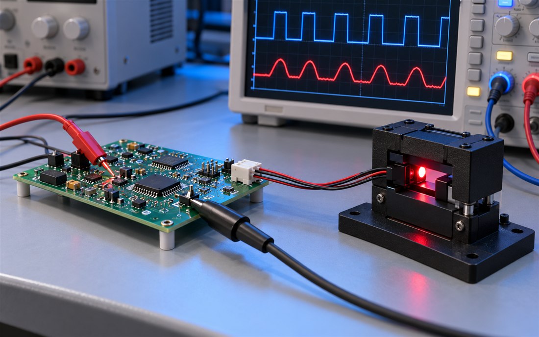
Use acceptance criteria defined by the product owner and applicable design controls. Recheck the sensor interface after changes to the AFE, LED, photodiode, cover, adhesive, solder mask, copper finish, or board geometry. The Healthcare PCB release package should include the stackup, optical keepouts, aperture dimensions, connector pinout, BOM, approved alternates, assembly drawing, and inspection notes. A PCB prototype assembly can expose access and fit issues before production files are frozen. A PCB engineering review can link verified observations to manufacturing controls. A PCB prototype verification step can compare the revised build with the documented baseline.
For the Healthcare PCB, preserve separation between LED pulse current and the photodiode receiver, coordinate analog timing with power behavior, and treat optics and mechanics as parts of the measurement chain. Verify the complete Healthcare PCB configuration and document every test condition. A PCB assembly process is only as repeatable as its drawings, BOM, inspection plan, and controlled configuration.
Sources: Texas Instruments AFE4404 product information and data sheet, for one specific wearable optical AFE implementation; Analog Devices, How to Design a Better Pulse Oximeter, for optical LED and photodiode signal-path considerations; U.S. FDA Electromagnetic Compatibility of Medical Devices Guidance, for device-level EMC context. No clinical performance or regulatory conclusion is claimed.

