
When a PLC cabinet starts producing false inputs, the root cause is often not the ladder logic. A 24 V field cable enters beside a noisy output, the protection network returns through a narrow trace, and the isolated logic ground is forced to absorb the event. An Industrial Automation PCB used for remote I/O, valve control, or a safety-adjacent interface needs a layout that makes those currents predictable before the board reaches the DIN rail.
An Industrial Automation PCB review should begin with the field cable, enclosure datum, and service expectation before routing is frozen.
This article addresses a common project failure: the schematic passes bench testing, but the assembled controller resets or misreads a sensor after a long cable is connected. The solution is a release method that aligns field protection, galvanic isolation, connector mechanics, and the manufacturing evidence needed for a repeatable build.
- Locate the field transient zone at the real terminal datum.
- Keep noisy 0 V and quiet logic reference paths intentionally separated.
- Choose isolation, creepage, and component placement as one design decision.
- Verify the complete cable-and-board interface with a controlled fixture.
Table of contents
For an Industrial Automation PCB, the field-side current path is a functional requirement, not a drawing annotation.
Put the field-side current path on the drawing
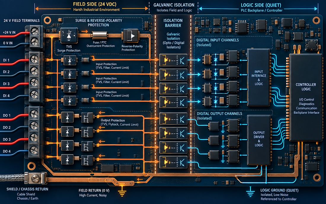
The first review of an Industrial Automation PCB should begin at the connector, not at the microcontroller. Mark the +24 V terminal, field 0 V, cable shield or chassis point, and the direction of the protection current. TVS parts, fuses, reverse-polarity devices, and input filters should be physically ordered by that current path. A schematic symbol placed far from the terminal cannot provide the same protection as a short copper route that reaches the intended return without crossing the logic area.
The Industrial Automation PCB output zone should be reviewed with the actual inductive load and cable length.
Where a machine has inductive loads, the output channel needs its own flyback or clamp strategy. Do not let a shared clamp trace run under a sensor reference or an ADC channel. The PCB materials and copper-balance choice also influence how much heat the protection and output devices can spread into the board. Use a copper region that the fabricator can reproduce, and call out any heavy-copper or thermal-via assumption in the manufacturing drawing.
Do not use the cable shield as a substitute for 0 V
An Industrial Automation PCB must keep shield current, field return current, and logic reference current distinguishable.
A shield can provide a low-impedance high-frequency path to the cabinet, but it is not automatically the return for a 24 V load. Bond the shield or drain wire to the chassis at the intended entry point, then define how field 0 V is referenced to the controller. The distinction matters when a motor contactor switches nearby: shield current should not be forced through the same copper neck used by sensor thresholds.
A high-frequency PCB mindset is useful here even for low-speed I/O. Fast edges from relays, PWM outputs, and cable capacitance create high-frequency current loops. A compact return, a controlled connector pinout, and a sensible via fence usually provide more margin than adding a filter after the board has already failed in the cabinet.
An Industrial Automation PCB becomes easier to qualify when the isolation boundary is visible to design, manufacturing, and service teams.
Make the isolation barrier visible to every team
Optocouplers, digital isolators, isolated DC/DC converters, and safety capacitors are not interchangeable graphical blocks. Draw the barrier through the PCB and into the enclosure. Mark the creepage direction, the clearance boundary, the slot or cutout if one is required, and the surfaces that must remain clean after assembly. A PCB manufacturing partner needs these features on the controlled fabrication data, while the assembler needs them on the inspection and coating instruction.
Leave a deliberate quiet side for the controller, clock, ADC reference, and communication transceiver. If an isolated converter returns its switching current through the wrong plane, the logic side may pass a static test but fail when the field output changes state. Put test pads on both sides of the barrier so the production fixture can verify the intended nets without bridging the safety distance.
Use the component package and mounting hardware as constraints
Isolation distance is affected by package body, lead geometry, solder mask, board edge, mounting hardware, and contamination. A narrow keep-out around an optocoupler is not enough if a metal standoff enters the same region. The PCB assembly traveler should identify polarity, orientation, barrier keep-outs, and any no-clean or cleaning requirement that affects insulation performance.
For a controller installed in a humid plant, conformal coating may improve environmental robustness, but it cannot be used to erase an undersized creepage path. The design must first meet the applicable safety intent with geometry; the coating is then reviewed through the assembly process for coverage, rework, and inspection. This order prevents a late process change from masking the actual design risk.
In an Industrial Automation PCB, channel grouping must balance noise, heat, and troubleshooting access.
Route I/O channels for noise, heat, and service access
Group channels by electrical behavior rather than by connector pin order alone. Fast outputs, relay drivers, and inductive loads should not share a narrow reference neck with high-impedance sensor inputs. Place the return vias next to the device that changes current, and give the logic side a defined reference transition. The fabrication release should include the layer stack, drill table, copper weights, and controlled impedance notes only where they are actually required; unnecessary tolerances make a build harder to review.
Heat is another source of field error. A protection diode or output transistor can warm the board locally, changing threshold or offset in an adjacent analog channel. Use copper spreading and thermal vias where the process can support them, but keep hot copper away from the precision reference. A surface finish choice should also match connector wear, soldering, storage, and corrosion exposure rather than being selected as a default.
Design for panelization and troubleshooting
The edge connector, terminal block, and test access must survive panel routing and depanelization. Put fiducials where the assembly machine can see them, keep tooling rails clear of service contacts, and reserve probe access for the field-side and logic-side supplies. A Industrial Automation PCB should inspect the panel drawing, not only the single-board Gerbers. If the board will be repaired, mark polarity and channel identifiers so a technician can diagnose a wiring error without a schematic viewer.
Keep thermal relief, solder mask openings, and connector footprints consistent with the assembly capability. If a board edge must mate with a DIN carrier or shield spring, show the mechanical datum and finish requirement in the same revision package. A nominally equivalent connector can move a contact by a fraction of a millimeter and change the service clearance or shield path.
An Industrial Automation PCB is not validated by a short jumper alone; the cable, load, shield, and enclosure are part of the test.
Validate the board with the cable and load attached
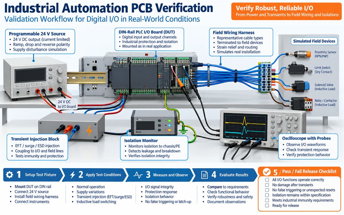
Bench tests with short jumpers do not represent a machine. Build a fixture that uses representative cable length, shield termination, inductive load, and enclosure ground. The fixture should be able to apply supply ramp, drop, reverse polarity, and transient conditions within the approved engineering plan. It should also observe input thresholds, output behavior, resets, and isolation status. A prototype PCB is valuable only when its mechanical and cable interfaces match the intended production build.
Turn observations into production gates
For an Industrial Automation PCB, each validation observation should map to an owner, a limit, and a disposition rule.
Record each check as a decision rather than a vague pass comment. Confirm that the field clamp returns to the expected chassis point, that the isolated side remains quiet during an output transition, and that no component or connector exceeds the agreed thermal or mechanical limit. The assembly fixture must carry the board revision and channel map so a fixture from an earlier design cannot silently approve a changed pinout.
| Release gate | Question to answer | Evidence |
|---|---|---|
| Field protection | Does the surge and clamp current return at the cable datum? | Layout review and fixture observation |
| Isolation | Are clearance, creepage, slot, and test access consistent? | Controlled drawing and inspection points |
| Thermal behavior | Can hot output parts avoid the precision reference zone? | Design target and thermal inspection plan |
| Serviceability | Can a technician identify and probe each channel? | Assembly drawing and troubleshooting map |
Freeze the I/O contract before volume purchasing
The Industrial Automation PCB purchase release should preserve the approved pinout, isolation, and fixture assumptions.
Before releasing the next lot of an Industrial Automation PCB, freeze the connector pinout, cable shield rule, isolation boundary, coating intent, and test fixture. A component alternate may have the same electrical rating but a different package, creepage path, thermal pad, or pin order. Attach the approved PCB manufacturing data and the Industrial Automation PCB assumptions to the purchase release so a buyer can evaluate substitutions without reopening the entire design.
An Industrial Automation PCB release is production-ready when the field current path, quiet reference, and isolation boundary are understandable to design, manufacturing, quality, and service teams. That shared picture is what keeps a cabinet problem from returning as a software mystery. A controlled pilot build confirms that the I/O contract is practical before volume purchasing.
The Industrial Automation PCB handoff is strongest when every team can identify the same return path and barrier boundary.
Sources: Analog Devices industrial interface and isolation application guidance; Würth Elektronik connector, grounding, and assembly notes; Qorvo transient and RF-interface references; protection, isolation, terminal-block, and PCB material supplier application data. The diagrams are original conceptual engineering graphics and do not represent a customer measurement or qualification report.
