
Table of Contents
A connected thermostat, lighting hub, or security gateway can pass a radio check on an open bench and still lose range after it enters a plastic enclosure. The usual cause is not one bad module. It is the interaction between antenna keep-out, shield hardware, switching regulators, clock harmonics, cable exits, and the return path on the Smart Home PCB. A practical design makes those interactions visible before tooling and firmware are frozen.
Why radio coexistence begins in the layout
Smart-home gateways often place Wi-Fi, Bluetooth, Thread, Zigbee, and a sub-GHz interface on one board. Each radio needs a controlled feed, a stable reference plane, and enough physical separation from noisy digital or power regions. The first Smart Home PCB review should mark each antenna aperture, feed transition, ground boundary, shield can, and connector datum. The enclosure drawing for a Smart Home PCB must be reviewed at the same time because a screw boss or metal insert can detune an antenna.
An antenna keep-out is more than a rectangle on the top layer. It includes the volume above the radiator, the ground pattern beneath it, nearby copper on adjacent layers, and the distance to a cable or battery. A radio keep-out drawing gives layout and mechanical teams one reference instead of separate assumptions. If a board edge moves, the feed length, return current, and enclosure clearance must be reviewed together.
Use the material stackup to control the feed geometry. A stable dielectric thickness and copper definition make the impedance target manufacturable, with a stackup-release check before fabrication, while an uncontrolled solder mask or connector launch can introduce a larger discontinuity than the antenna itself. For a production Smart Home PCB, freeze the stackup and launch details before the radio team tunes matching components.
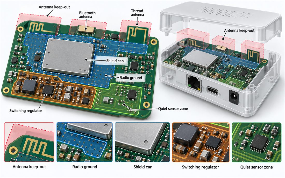
This conceptual graphic shows antenna keep-outs, radio ground, a shield can, switching regulator, and quiet sensor zone. It is a design explanation, not a measured customer board. Use a low-loss material review when the gateway must retain margin across temperature, enclosure variants, and production tolerances.
Keep switching noise away from the antenna
A regulator can be electrically efficient and still create a difficult RF problem. Its inductor node, clock edge, and return current can couple into an antenna feed or sensitive crystal. Place the power stage so the high di/dt loop is compact, keep its return local, and prevent it from crossing the radio reference. A power-noise boundary on the layout gives the design reviewer a physical rule to enforce.
Shield cans are useful only when their seams, vias, and grounding points are intentional. A shield that floats at one corner can become a resonant structure. A dense via fence can improve containment, but it must not cut the antenna return or create a narrow neck in the main plane. Check the shield footprint, solder mask, and rework access with assembly inspection before releasing the stencil.
Keep the digital clock, Ethernet or USB connector, and sensor front end out of the antenna current path. A ground-return inspection should verify actual copper and via continuity rather than relying on a net name. The same inspection should confirm that a late component alternate does not move a noisy return underneath the radio feed.
Verify the gateway as a system
Bench verification should use the intended enclosure, cable arrangement, firmware modes, and power source. A loose wire antenna and an open board can hide the interaction that appears after installation. Define an RF fixture datum that locates the board, antenna port, shield hardware, and enclosure without bending the board or changing connector pressure.
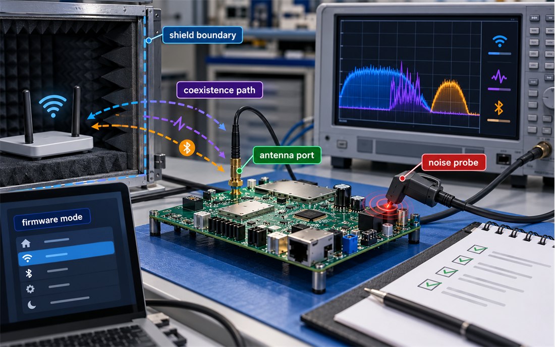
The second conceptual image shows a coexistence path, antenna port, shield boundary, noise probe, and firmware mode. The spectrum display is illustrative and contains no measured values. Use a coexistence test matrix to vary one condition at a time: radio duty cycle, processor load, power mode, enclosure state, and cable position.
Record the board revision, module lot, antenna part, enclosure revision, firmware build, and fixture serial with each result. If a range complaint appears in production, this record helps the team separate a layout change from a firmware or enclosure change. A configuration traceability log is often more valuable than a single impressive bench plot.
Release rules for a connected product
Project managers should release a gateway with a controlled package: stackup, antenna drawing, keep-out, matching BOM, shield and via-fence details, connector datum, enclosure interface, fixture setup, and acceptance criteria. A radio-assembly traveler should identify orientation, shield solder coverage, connector seating, and the inspection points that affect RF performance.
- Freeze antenna aperture, feed, ground pattern, and enclosure datum together.
- Keep high di/dt power loops outside the radio return path.
- Inspect shield seams, via fences, connector launches, and solder coverage.
- Repeat coexistence checks after firmware, enclosure, module, or antenna changes.
- Link each unit to a board revision, fixture revision, and approved configuration.
A reliable Smart Home PCB is the result of coordinated RF, mechanical, power, and assembly decisions. The goal is not to promise one universal range number. The goal is a board and release process that preserves the intended radio margin when the product leaves the bench and enters a real home.
Make the enclosure handoff auditable
The Smart Home PCB should be released with the enclosure, antenna, shield, and firmware assumptions visible in one package. The production Smart Home PCB record should identify the board revision, antenna part, matching network, fixture, and firmware mode used for the accepted check. If a plastic wall, metal screw, cable, or power adapter changes, the same package tells the team what must be repeated before shipment.
This handoff also protects purchasing and service teams. An approved alternate is not just a similar radio module; it must preserve feed geometry, ground reference, thermal behavior, and inspection access. A Smart Home PCB change record makes that review explicit instead of leaving range problems to field returns.
Sources: Analog Devices mixed-signal and RF layout guidance; Würth Elektronik EMC, shielding, and assembly notes; Qorvo wireless front-end integration references; antenna, connector, and laminate supplier data. Values above are engineering practices or design targets, not customer measurements.
