
Table of Contents
A long outdoor cable turns a LoRa PCB into more than a radio layout. The coax connector, chassis wall, cable shield, mounting hardware, and surge path become part of the RF and reliability system. A board may tune correctly on a short bench cable but lose sensitivity when the final harness is installed, or reset when an electrostatic discharge finds a low-impedance path through the receiver ground. The practical fix is to release the coax launch, return current, and protection path as one controlled interface.
Why a cable launch changes the board problem
The cable carries the wanted signal, but it also brings an external reference into the enclosure. If the connector shell is floating, return current may cross a digital ground split before reaching the chassis. If the shield is bonded far from the entry point, the cable becomes an unintended radiator. A LoRa PCB review should therefore map three paths separately: the RF signal path, the normal RF return path, and the short ESD or surge path that should bypass sensitive circuitry.
Start with a mechanical datum. The connector center, enclosure wall, shield bond, and first return via should be dimensioned together. Use a coax launch geometry review to prevent the connector from being placed by a generic library footprint that ignores the chassis cut-out. The feed line should leave the connector without a sudden reference-plane change, and the mounting pads should not force the board to flex when the cable is tightened.
Build the coax transition around a LoRa PCB return path
At the launch, signal continuity is only half of the design. The return current wants a low-inductance route around the signal via or pad. Place the first return vias close to the launch, keep the reference plane continuous, and avoid an isolated copper island under the connector. When the board is multilayer, document which plane owns the transition and how the connector shell reaches the chassis. A short, direct return-via field is easier to inspect than a broad pour whose current path changes with every revision.
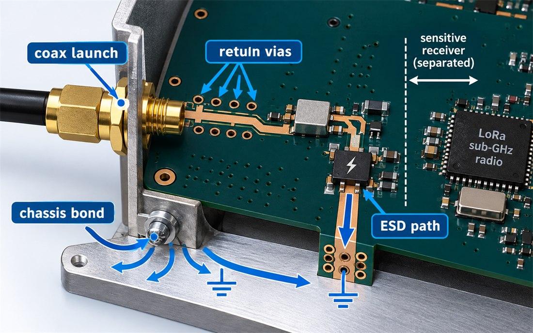
This conceptual figure shows a coax launch, return vias, chassis bond, and ESD path. It is an engineering explanation, not a measured insertion-loss plot. For a production LoRa PCB, the laminate and copper specification should be locked before tuning. A change in dielectric thickness, copper roughness, or plated-hole geometry can move the launch impedance even when the top-layer drawing looks unchanged.
Keep the connector footprint mechanically honest
Connector drawings often specify shell tabs, solder fillets, and mounting posts that are absent from a simplified RF footprint. Include those features in the mechanical view and show the cable bend envelope. The chassis bond should not depend on a thin solder bridge that can crack during cable service. If a press-fit or edge connector is used, define the plated-hole or edge geometry, support condition, and acceptable burr level in the fabrication notes.
Separate ESD energy from the receiver
Protection components are effective only when their current path is shorter and lower impedance than the path through the radio ground. Put the entry protection near the connector, give it a defined chassis destination, and keep the protected node away from the low-noise receiver matching network. A ESD protection placement review should include the component footprint, pad-to-chassis spacing, solder-mask opening, and the assembly sequence. Do not move a suppressor during layout cleanup without reviewing the current path again.
The shield and chassis strategy also affects cable noise. A cable-shield termination can be bonded directly at the entry wall, through a controlled spring contact, or through a connector shell. Each choice changes the RF reference and the service behavior. The enclosure datum should identify where the shield is expected to touch, while the PCB drawing identifies the copper and via features that support that contact.
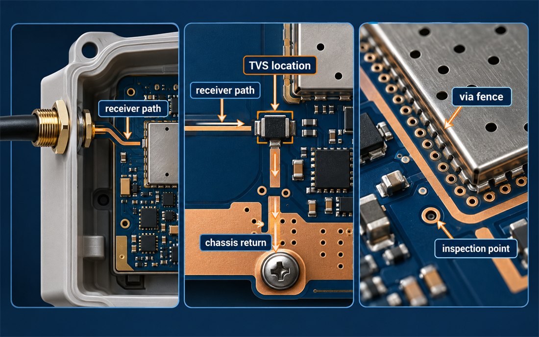
The second conceptual figure separates the receiver route from a chassis discharge route and shows an inspection point at the connector. It does not represent a customer test result. During a release, verify that the ground-fence inspection checks actual via presence, annular-ring quality, and solder-mask clearance rather than only confirming that the CAD layer exists.
Verify the assembled cable interface
Bench RF checks should use the final connector, cable type, enclosure wall, and mounting hardware. A short jumper can hide a shield-current problem; a long harness can expose it. Record cable routing, bend radius, connector seating, and the chassis contact condition. Add connector torque control to the assembly traveler when a threaded connector is used. Excessive torque can bow the board; insufficient torque can leave the shield discontinuous.
Inspect the finished LoRa PCB before attributing a sensitivity change to the radio IC. Check the launch solder fillet, plated holes, via fence, mask slivers, and any exposed copper at the enclosure edge. A creepage and clearance review should also confirm that the protection path has the intended spacing after coating or cleaning. The acceptance method can be a drawing check, a continuity check, or a defined RF comparison, but its boundary must be stated.
Release a LoRa PCB cable interface for production
- Freeze connector center, enclosure wall, chassis contact, and first return-via locations in one controlled datum.
- Show RF signal, normal return, shield, and ESD paths on the same interface drawing.
- Keep the launch reference plane continuous and document the approved laminate and copper construction.
- Define connector support, cable bend envelope, torque or insertion condition, and fixture contact points.
- Inspect plated holes, via fence, solder mask, shell bond, and protection footprints at first article.
- Record any cable, connector, enclosure, coating, or protection substitution in the change-control record.
The final LoRa PCB traveler should name the approved cable, connector, and protection revision. When those controls are released together, a LoRa PCB is easier to install, troubleshoot, and reproduce. The objective is not to claim a universal range or immunity number. It is to make the cable interface predictable enough that RF tuning, ESD protection, and manufacturing inspection support the same product decision.
Sources: Taconic RF laminate technical data and application guidance; Würth Elektronik connector and RF transition notes; Analog Devices grounding and ESD layout guidance; Qorvo front-end and antenna integration documentation. Values and checks above are engineering practices or design targets, not customer measurements.
