
An Aluminum Nitride PCB sensor carrier must keep package geometry, RF return, and thermal margin visible in one controlled interface drawing.
An mmWave sensor carrier must keep the feed geometry stable while moving heat away from the active device and preserving the enclosure datum. Aluminum nitride can support that combination, yet the first build can still drift when a cavity, lid, connector, adhesive, or copper spreader is released separately. The most useful review treats the carrier as an RF, thermal, and mechanical part rather than a passive board.
Freeze the package datum
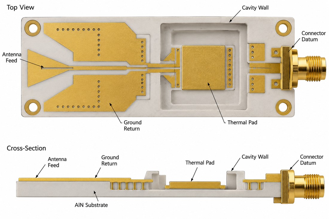
Start with the antenna aperture, connector axis, cavity wall, mounting holes, and thermal interface. The Aluminum Nitride PCB substrate should have a controlled edge or metallized boundary wherever the field depends on it. Keep the RF datum separate from the enclosure datum until the tolerance stack is closed, then document how the two are related.
The thermal management design review should show lid spacing, bond-wire or package keep-out, adhesive limits, and every metal feature near the feed. Mark which dimensions are electrical, mechanical, and inspection-critical. A small connector offset can matter more than a long low-loss trace.
Keep thermal copper outside the sensitive aperture unless the electromagnetic boundary has been reviewed. A heat spreader that changes the local dielectric or ground boundary is an RF change.
Build return and thermal paths together
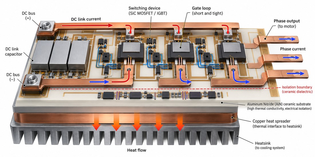
Place ground vias or metallized walls close to the feed and show the current loop through the carrier and enclosure. The Aluminum Nitride PCB layout should identify where the return crosses layers and where a thermal via array is allowed to share the region.
The thermal interface needs its own flatness, pressure, and support specification. The RF PCB manufacturing note should identify copper construction, attach method, inspection access, and the permitted seal or coating around the sensor aperture.
Use geometry correlation before tuning the circuit. Record cavity, connector, and lid dimensions under a defined fixture, and keep measured evidence separate from the design target.
Release the sensor module as one assembly
The package should contain the stack or cross-section, aperture drawing, RF launch, thermal interface, assembly sequence, cleaning limits, and acceptance plan. The controlled impedance handoff should state whether the evidence is dimensional, electrical, thermal, or visual.
If the enclosure, connector, or carrier changes, repeat the affected geometry and return-path review. Do not tune a prototype to a cavity that procurement cannot reproduce.
Use a final checklist: datum chain, ground boundary, thermal contact, connector coplanarity, seal keep-out, and revision-controlled material data.
An Aluminum Nitride PCB sensor carrier succeeds when the aperture, return path, heat path, and enclosure datum are released together. Correlate the fabricated geometry before interpreting mmWave performance.
For project control, record the interface owner, drawing revision, supplier capability note, and the exact condition that would reopen the review. A clear decision log is especially useful when a sourcing change, enclosure change, or assembly change arrives after the RF model has been signed off. The team can then distinguish a harmless documentation update from a change that requires a new coupon, cross-section, or environmental check.
Engineering release note: keep the thermal interface, RF reference, and inspection datum visible in the same revision-controlled package. When a device, copper feature, carrier, or assembly step changes, identify the affected assumption and repeat only the evidence tied to that boundary. This prevents a typical material value from being mistaken for a guaranteed product result.
Release note: keep the Aluminum Nitride PCB sensor-carrier geometry, return path, and thermal margin visible in the interface-control drawing.
Sources: CeramTec aluminum nitride substrate data; Analog Devices RF and mixed-signal PCB layout guidance; supplier application notes for direct-bond copper and high-power ceramic modules. Numerical values are treated as typical supplier values, design targets, or engineering ranges unless a released drawing defines a measured acceptance value.
Release gate: document the Aluminum Nitride PCB interface before approval.
Release gate: document the Aluminum Nitride PCB interface before approval.
Release gate: document the Aluminum Nitride PCB interface before approval.
Release gate: return the PCB manufacturing evidence with the lot package.
Release gate: return the PCB assembly evidence with the lot package.
